PCB Designer
-
Routing Without Nets
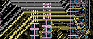
In high-density, multi-layer, high-pin-count designs, using "Routing Without Nets" reflects design intent flexibly and efficiently.
-
Coil Routing Wizard
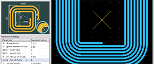
Using the wizard, you can instantly and automatically generate the uniform coil routing essential for compact and high-frequency PCB designs.
-
-
Export for Transmission Line Analysis
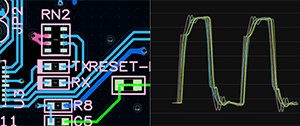
By exporting DSN files, Quadcept enables smooth integration with various simulators, such as DEMITAS NX and SIGNAL ADVISER.
-

-
Panelization
In addition to multi-imposition of identical boards, multiple panelization of different board designs is now supported.
-
-
Mesh Copper Pour
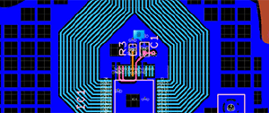
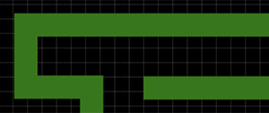
Create meshed copper pours effortlessly to comply with UL standards or requirements for transparent substrates.
-
-
Sharp-Corner Routing
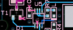
Enables sharp-corner routing commonly used in high-frequency designs. Trace end caps become square corners, and routing angles can be set to 90 degrees or customized as needed.
-
-
DFM Manufacturing Check (MRC)
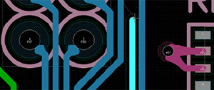
Performing manufacturability checks during PCB design eliminates wasteful rework during board manufacturing. Quadcept continuously enhances its DFM Manufacturing Check (MRC) features—a capability not found in low-cost CAD tools.
-
-
Online DRC
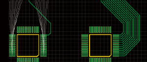
Verify clearance and design rules in real time as you layout traces, eliminating rework and improving overall design quality.
-
-
Semi-Automatic / Push / Hug Routing
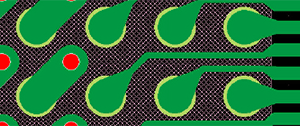
To support high-speed routing, differential pair routing and trace length control can be easily performed using DRC design rules. Additionally, it supports push routing and hug routing that minimize clicks to the extreme, as well as semi-automatic routing that automatically searches for the shortest path.
-
-
Design Rule Areas
Add custom DRC rules to high-density areas like BGA surroundings that standard DRC cannot handle, reducing time-consuming visual checks. Directly apply special settings for trace widths, clearances, and via shapes.
-

-
ODB++ Export
Supports the integrated ODB++ database format to reliably convey information from PCB design through manufacturing and assembly. It can be used for global data communication across companies.
-
-
Automated Test Point Generation
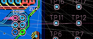
Automatically generate a test point for each net and place them sequentially, removing the tedious manual setup process.
-
-
Design Difference Comparison
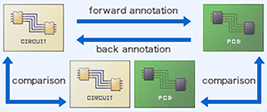
Compare design revisions across multiple domains, including Schematic-to-Schematic, Schematic-to-PCB, PCB-to-PCB, and PCB-to-Schematic for error-free forward/back-annotation and revision control.
-
-
Keepout Areas / Component Areas
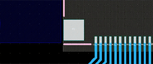
Define keepout areas—component height, drill placement, and net keepouts—during footprint creation or PCB design to detect them as DRC errors. Custom component areas with height data can also be added and exported to IDF.
-
-
Board Edge Slit Input
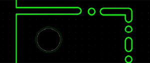
Added a feature to quickly enter slits—for creepage distance, board outline, or panelization mouse bites—as if drawing standard lines, replacing time-consuming line and arc combinations.
-
-
Component Wizard (IPC Compliant)
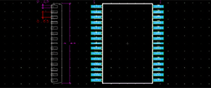
Entering IPC standard values for high quality and reliability in assembly allows the component wizard to automatically generate pad placements, courtyard outlines, dimension lines, and silkscreens. This feature enables a significant reduction in component creation time.
-
-
Flexible Copper Pour
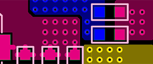
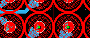
Features automatic thermal generation, real-time clearance updates around obstacles, and automatic island removal for power/GND reinforcement copper, inner-layer copper, and automatic top-layer copper, enabling speedy copper editing.
-
-
Design Rule Check
In addition to per-net rules, DRC grouped by net classes is available. Users can customize DRC by freely registering target items, values, and layers—such as silk-to-solder mask or mask-to-pattern—for manufacturability.
-
-
Offset Shape Creation
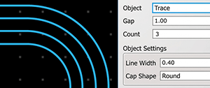
Generates concentric objects while maintaining center coordinates. It is useful for creating keepouts around mounting holes or temporarily arranging evenly spaced traces with fixed clearance to check routing space.
-
-
Automatic Assembly Drawing Generation
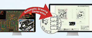
Automatically generates assembly drawings from PCB placement data, reflecting polarity, component values, and unmounted settings, with batch output per layer. Fully linked with design data, it eliminates manual drawing and transcription errors to quickly produce accurate drawings.

-
-
Electrical and Mechanical Integration in a 3D Design Environment
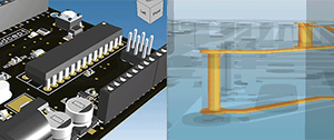
Smoothly handles enclosure import and PCB alignment in CAD. Its high-speed viewer enables accurate interference checks using manufacturer 3D models as-is. It also supports integrated STEP export for PCBs, components, and enclosures together.
-
-
S-NAP® (Electromagnetic Field Simulator) Integration
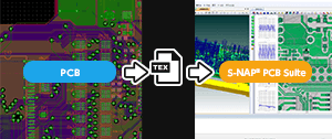
Supports TEX file export for S-NAP® PCB Suite. Specifying power/GND nets and Value attributes eliminates extra work after data input.