

Quadcept : Creating Footprints
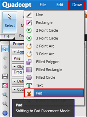
STEP 2: Place Pads
Pads are land shapes for electrically connecting PCB component terminals.
The following will explain how to place pads.
| Placing Pads |
| Place a component pad. |
|
 |
|
 |
|
 |
|
 |
Pad
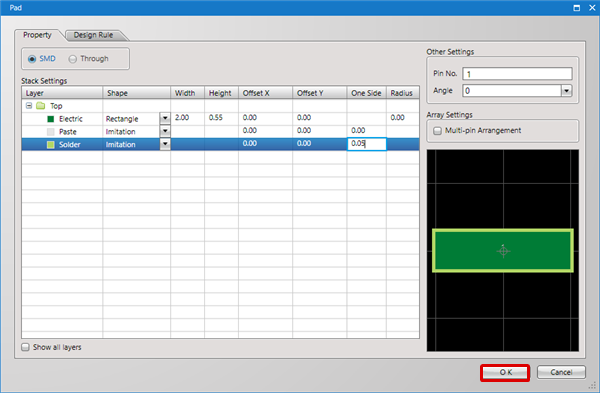
Pad Type
| Type | Content |
|
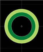
SMD |
Pad without a hole. Pad shape for surface mounted components such as Chip components. |
|
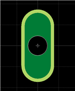
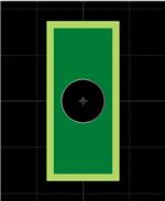
Through |
Pad with a hole. Pad shape for through hole mounted components such as Dip components. |
Layer Settings
| Item | Content |
|
Top |
Sets the land size of the Top surface. |
|
Inner |
Sets the land size of the Inner layer. (For the Inner layer, all are the same size.) |
|
Bottom |
Sets the land size of the Bottom surface. |
Layer Type
| Item | Content |
|
Electric |
Sets the copper layer. These are land settings. |
|
Paste |
Sets the area where paste solder is applied. |
|
Solder |
Sets the solder resist area. |
Land Settings
| Item | Setting Contents | Content |
|
None |
None |
|
|
Circle |
Width (Diameter) |
|
|
Square |
Width Radius |
|
|
Oval |
Width Height |
 |
|
Rectangle |
Width Height Radius |
|
|
One Side (One Side over size) |
Settings can be configured based on the size of the land (Electric layer). |

When a Radius is input for a Square or Rectangle, you can specify the roundness of a square pad.

Drill Settings
* This can only be set when "Through" is selected as the pad type.
| Item | Content | ||||||||
|
Shape |
Sets the drill shape and size.
W: Width |
||||||||
|
Tolerance |
Sets the tolerance for the drill diameter. This is shown for NC Drill Files and Print NC Drill Lists. |
||||||||
|
Plating |
Possible to set whether to plate a hole. Normally, "Plating" should be checked for component pads. |


Other Settings
| Item | Content |
| Pin No. |
Specifies the Pin No. |
|
Angle |
Specifies the Angle. |
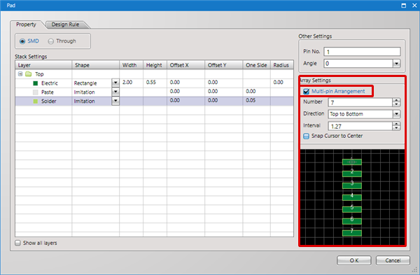
Multi-pin Arrangement
When Multi-pin Arrangement is enabled, multiple pads can be placed together by specifying the Number, Direction, and Interval for pad placement.
| Item | Content |
|
Number |
Specifies the number of arranged pads. |
|
Direction |
Select either "Top to Bottom", "Bottom to Top", "Left to Right", or "Right to Left". |
|
Interval |
Sets the pad-to-pad interval. |
|
Snap Cursor to Center |
Check for whether to place by snapping the cursor to the center of multiple pads. |
For more details about the pad sizes that our company uses, refer to "Reference: Pad Dimensions".