A Test Land, also referred to as a Test Pin or Test Point, is a point used for board electrical tests.
The following will explain the method for "Placing to Schematics and PCBs", and for "Placing to PCBs Only".
Create Test Points using a component, and then place them at arbitrary locations on both schematic drawings and PCB drawings.
With this method, it is an annotation target. |
| (1) |
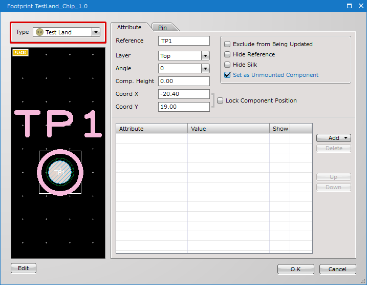
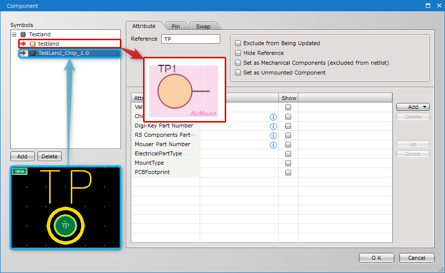
Register Test Pin shape symbols and Test Land footprints by creating a component.
Place a check next to "Set as Unmounted Component". |
|
 |
Test Lands can be placed as a batch to PCB drawings. (Create Test Land Automatically)
By having Test Land attributes, Test Lands are outside the annotation target for schematics. |