

Quadcept : About Quadcept
About Objects Used in Quadcept
Objects used in Quadcept are items and targets used (for drawing/editing) in Quadcept.
Objects used in Quadcept include the following.
The following will explain each item.
Common
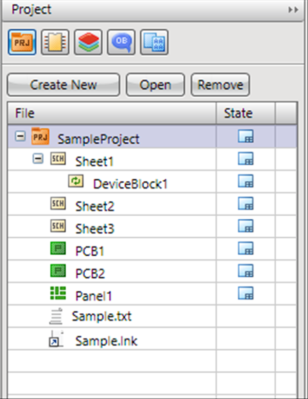
| Project |
| A Project is a file that manages schematics or design drawings for PCBs, etc. In Quadcept, schematic design drawings and design drawings for PCBs must have a Project as a parent. Schematics and PCBs stored in a project are paired so that you can confirm differences. |
|
|
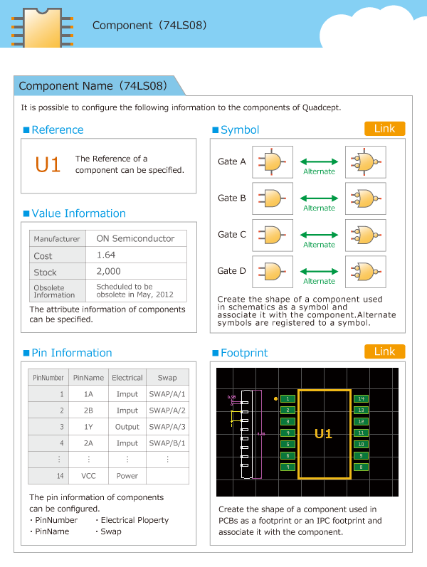
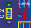
| Component |
| A Component is an object that can register "Symbols" that are shapes placed on a schematic, "Footprints" and "IPC Footprints" that are shapes placed on PCB design drawings, and "Attributes" such as the Maker and Price. By creating a Component, it becomes easy to link circuits and PCBs and manage components. |
|
|
Schematic
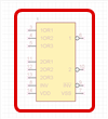
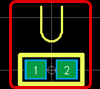
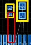
| Symbol |
| This is the shape placed on a schematic. The symbol itself can be placed on the schematic as is, and after configuring settings such as Attributes, by registering it to a component, it becomes possible to manage it as a component. |
|
|
| Pin |
| This is the shape of a pin connected to a wire. |
 |
| Pin Point |
| Among the pin shapes, this is the shape that expresses the portion that connects with the wire. This is shown when a wire is not connected, and it is automatically hidden once a wire is connected. When it is not connected, a "□" shape is shown, and when a pin is set to "Non Connection", an "×" shape is shown. |
 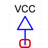 |
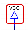
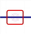
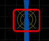
| Power Supply |
| The power supply is the shape for expressing the voltage reference point. |
|
|
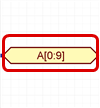
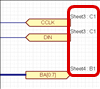
| Port |
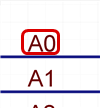
| This is the destination port used when wires on the schematic extend to another sheet, or when there is not enough space for creating wiring on the schematic. It can also be used for specifying the Net Name. |
|
|
| Port Address |
| This is the object that indicates the address and sheet for the port connection destination. The connection location is automatically shown using Update Port Address. |
 |
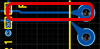
| Wire |
| An electrical line that connects pins to pins in a component. Information connected by wires becomes a Netlist. |
 |
| Junction |
| This is an object that integrates intersecting wire nets at wire junctions. Wires that are connected at junctions become the same net. |
|
|
| Bus |
| It is possible to integrate wires pulled from ICs, and FPGAs, etc. For a bus, when wires are connected, it is possible to make a ripper (skew wire) occur automatically. |
|
|
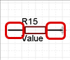
| Label |
| For wires, it is possible to specify the Net Name. |
|
|
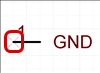
| Connection Point |
| A Connection Point is a function for setting one point as a reference potential also referred to as a "Single Point Ground" or "Single Point Earth". This is used when connecting an analogue circuit current to a different potential net such as a digital circuit current. A single junction can be placed separately for a schematic and PCB so that the consistency of the net information between the schematic and board can be ensured, and so that designing can done at board routing without showing unnecessary DRC errors. |
|
|
| Drawing Frame |
| This is the drawing frame a schematic. |
 |
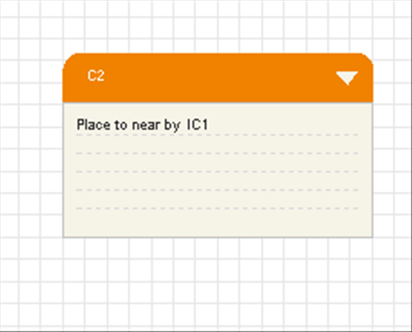
| Memo |
| Memo is a function for placing work-related comments by the designer on the schematic. It is possible to toggle display and printing ON/OFF according to each layer so that the intent of the designer can be properly passed on to each person in charge. |
   |
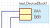
| Device Block |
| The Device Block is for executing common design of proven schematics created in the past. Past schematics can be applied similarly to placing components. |
 |
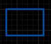
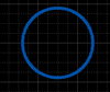
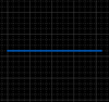
| Other Draw (Line/Rectangle/Circle/Arc/Text, etc.) |
| Various shapes can be drawn such as Lines, Rectangles, Circles, Arcs, and Text. |
    |
PCBs
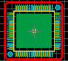
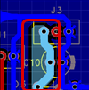
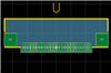
| Footprint |
| This is a shape placed on a PCB design drawing. The footprint itself can be placed on the PCB design drawing as is, and after configuring settings such as Attributes, by registering it to a component, it becomes possible to manage it as a component. |
 |
| IPC Footprint |
| This is a shape placed on a PCB design drawing.The difference with a footprint is that this is created automatically according to IPC standards by registering values in the Wizard. As with footprints, it can be placed on the PCB design drawing as is, and after configuring settings such as Attributes, by setting it to a component, it becomes possible to manage it as a component. |
 |
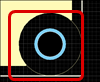
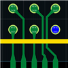
| Pad |
| Principally, this is used for locations where component pins are soldered and for mounting holes. |
 |
| Via |
| This is used for routes and for connections between layers such as planes. |
 |
| Rats |
| These indicate net connection information. |
 |
| Route |
| This draws the line where electrical signal lines flow based on the Rats (Net Information). |
 |
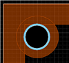
| Plane |
| The plane is the copper area on the board, and it is sometimes referred to as the Copper. Because it is the copper area, electrical signals flow the same as with Routes. However, Routes are linear shapes, whereas arbitrary shapes can be created for Planes allowing for Routes to be reinforced. In Quadcept, there are Dynamic Planes (in the drawn area, the plane that connects for automatically set Net Names, and for other nets, the shape is updated to maintain clearance) and Static Planes (planes that do not change shape). |
 |
| Thermal Line |
| The Thermal is a shape with a slit for preventing heat from spreading to Planes with wide areas for Pads on the same net as the created Plane. The Thermal Line becomes the connection line between the pad of the thermal shape's plane shape and Plane. This is automatically drawn using the Plane Settings, but it is possible to delete unnecessary lines later. |
 |
| Cutout |
| This is used for Planes, Polygons, and Keep Out Areas. The drawn area will become a partially cutout status inside the Plane/Polygon/Keep Out Area. |
 |
| Assembly Area |
| Sets the Assembly Area. This becomes the component data area at component clearance check with DRC and 3D export. |
 |
| Keep Out Area |
| This is the Keep Out Area for "Component Height Restriction", "Drill Placement Restriction", and "Restricted Net Restriction". In addition to visual confirmation, a check can be performed with DRC. |
 |
| Design Rule Area |
|
For the Design Rule Area, when the Design Rules differ according to the layer and area instead of for the whole board in the DRC Settings items, |
 |
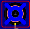
| Connection Point |
| A Connection Point is a function for setting one point as a reference potential also referred to as a "Single Point Ground" or "Single Point Earth". This is used when connecting an analogue circuit current to a different potential net such as a digital circuit current. A single junction can be placed separately for a schematic and PCB so that the consistency of the net information between the schematic and board can be ensured, and so that designing can done at board routing without showing unnecessary DRC errors. |
 |
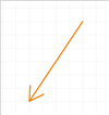
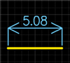
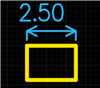
| Dimension |
| This indicates distances and angles using Arrows, Lines, and Text. There are various types of dimensions indicating Circle diameter, Line length, Angle, and Pad size. |
  |
| Other Draw (Line/Rectangle/Circle/Arc/Text, etc.) |
| Various shapes can be drawn such as Lines, Rectangles, Circles, Arcs, and Text. |
    |