The recommended route width can easily be calculated for routes that require impedance control.
From the Route screen, it is possible to confirm the "Recommended Gap" for Differential Pairs in addition to the "Recommended Width" for a Single End.
The Impedance value is the logical value based on the assumed margin of ±10%, so use this as the reference Gap value.
The measured value fluctuates according to the material, so confirm details with the planned board manufacturing factory.
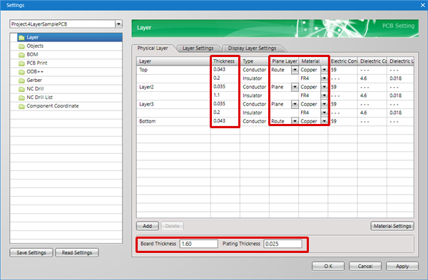
Preparation for Recommended Width Calculation
It is necessary to set the Layer Configuration in advance in order to calculate the Recommended Width and Recommended Gap.
| Item |
Content |
|
Layer Settings
|
Configures board layer settings.
Settings for Board Thickness, Plating Thickness, Plane Layer, Material, and Dielectric Constant are required.
|
| The following will explain how to calculate the Recommended Width for a Single End. |
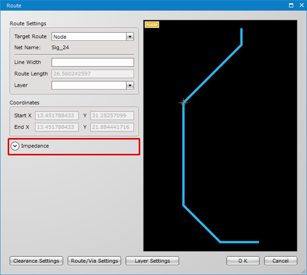
| (1) |
Double-click a route.
=> The Route dialog will be displayed. |
| (2) |
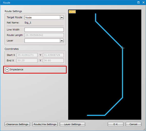
In the Route dialog, place a check for "Impedance".
=> Impedance setting items will be displayed. |
|
 |
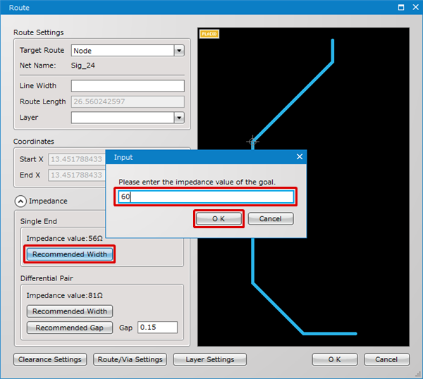
| (3) |
Click "Recommended Width".
=> The input screen for the Impedance desired value will open. |
| (4) |
Input an Impedance value, and then click "OK".
=> Here, "60" is input. |
|
 |
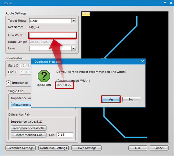
| (5) |
The Recommended Width will be displayed. Click "Yes".
=> The Recommended Width will be reflected to the Line Width. |
| |
|
| |
* The same operation is possible for calculating the Recommended Width for a Differential Pair. |
|
 |
| The following will explain how to calculate the Recommended Gap for a Differential Pair. |
| (1) |
Double-click a route.
=> The Route dialog will be displayed. |
| (2) |
In the Route dialog, place a check for "Impedance".
=> Impedance setting items will be displayed. |
|
 |
| (3) |
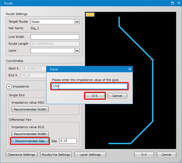
Click "Recommended Gap".
=> The input screen for the Impedance desired value will open. |
| (4) |
Input an Impedance value, and then click "OK".
=> Here, "100" is input. |
|
 |
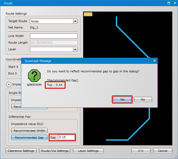
| (5) |
The Recommended Gap will be displayed. Click "Yes".
=> The Recommended Gap will be reflected in textboxes. |
| |
|
| |
* With the current version, it is not possible to reflect the Recommended Gap to PCB drawings, so adjust the interval manually. |
|
 |