

«
Cut Pad
|
Relative Move
»
PCB Layout CAD : Various Convenient Functions
Swap
It is possible to perform Swap Pin and Group Swap when designing a PCB by registering swap information to a component pad.
About Swap Registration, refer to Registering Swap Information.
The following will explain how to execute Swap using registered Swap Information.
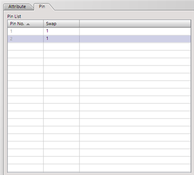
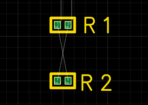
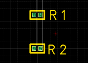
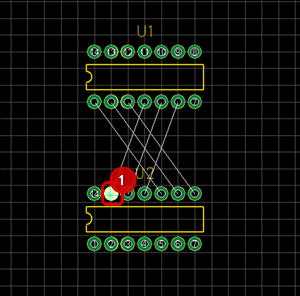
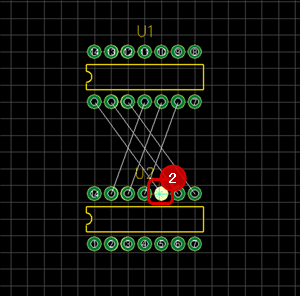
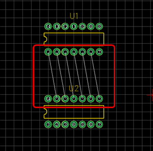
| Swap Pin is used for replacing Net connections between equal pins of Component Swap Information. By replacing Net connections, it is possible to improve route paths. |
|
|
|
|
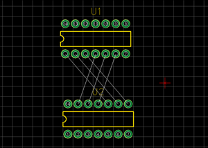
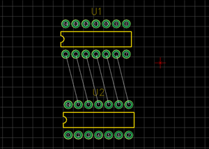
| Before Swap Pin | After Swap Pin |
|
|
|
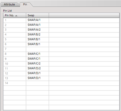
| Group Swap is used for replacing Net connections between equal pins of Component Swap Information where Group Settings have already been configured. By replacing Net connections, it is possible to improve route paths. |
|
|
|
|
| Before Group Swap | After Group Swap |
|
|
|
Swap Pin / Group Swap Rules
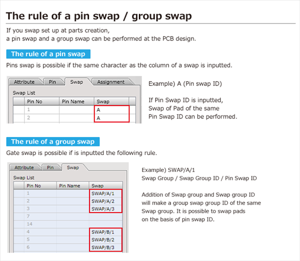
| Swapping |
| The following will explain how to execute Swap Pin and Group Swap. |
|
 |
|
 |
|
 |