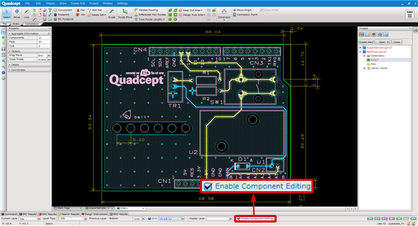
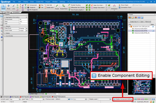
With the "Enable Component Editing" function, you can edit the objects in a footprint on a PCB/panel sheet during design. This is useful when you want to move a 1 pin mark or delete unnecessary silk overlapping with solder resist.
* The following objects cannot be moved or deleted.
- Pad
- Assembly Area (Move is allowed.)
- Reference (Move is allowed.)
| The following explains how to edit the silk in a footprint using the "Enable Component Editing" function. |
| (1) |
Check the checkbox of "Enable Component Editing". |
| |
=>The objects in a footprint will be editable. |
|
 |
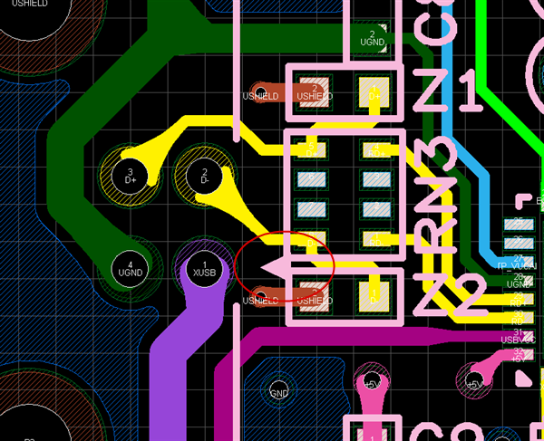
| (2) |
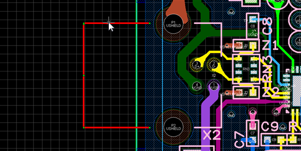
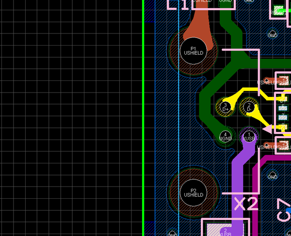
Select a 1 pin mark overlapping with the silk of other components. |
|
 |
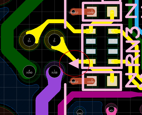
| (3) |
Move the mark to the location where the silk does not overlap. |
|
 |
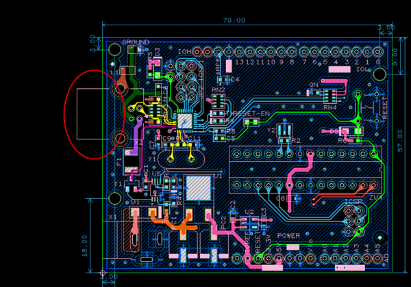
| Delete the silk which sticks out from board outline next. |
|
 |
| (4) |
Select the silk which sticks out from board outline. |
|
|
 |
| (5) |
Press the Delete key. |
|
| |
=>The selected silk will be deleted. |
|
|
|
| (6) |
After editing a component, uncheck the checkbox of "Enable Component Editing". |
|
| |
=>The component editing mode will be canceled. |
|
|
|
The component edited on a PCB sheet can be detected by the DRC item, "Edit Component".
For silk editing, the "Subtract" function allowing you to cut objects is useful.