The layers need to be assigned for the conversion since the configuration of the layer information between Quadcept and CR-5000 Board Designer is different.
Assignment information can be saved, and its settings can be read and used for the same layer assignment.
The following will explain how to assign the layer information of CR-5000 Board Designer to the one of Quadcept.
Assigning layers
Releasing assigned layers
Saving assignment settings
Reading assignment settings
Layer settings
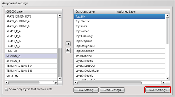
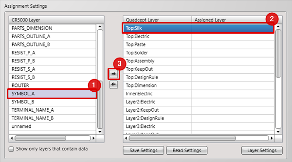
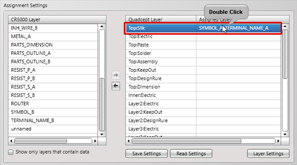
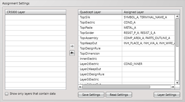
| The following will explain how to assign layers on the Assignment Settings. |
| (1) |
Select a layer you want to assign from the CR5000 Layer. |
| (2) |
Select a layer from the Quadcept Layer to assign the selected layer on (1) to. |
| (3) |
Click the "->" button. |
|
 |
| |
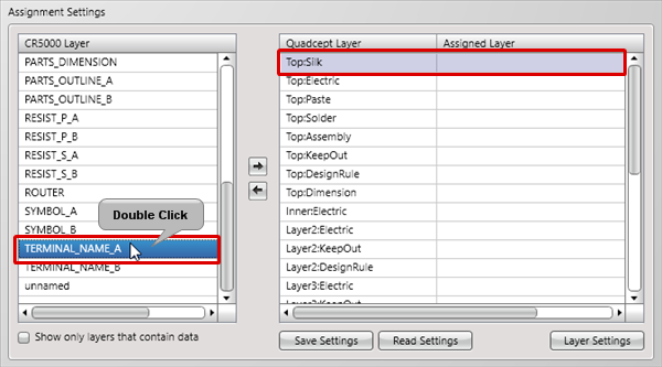
*The layer can also be assigned by double-click. |
|
 |
| |
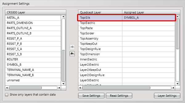
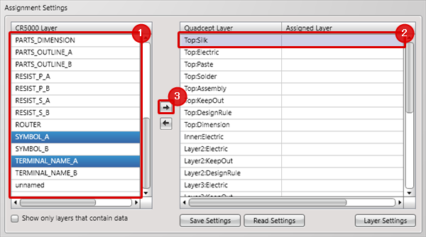
It is also possible to assign multiple layers together
by selecting layers while pressing Ctrl or Shift key. |
|
 |
|
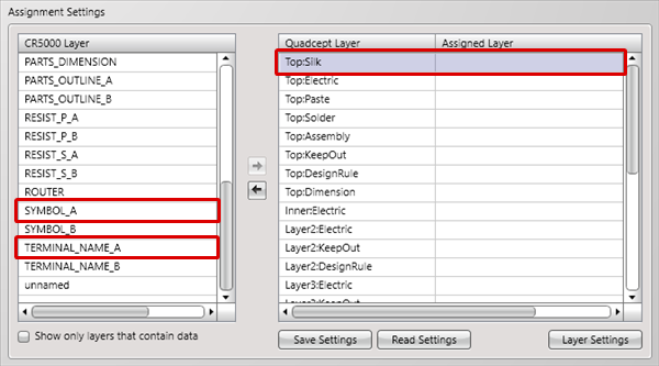
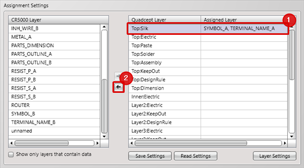
The following will explain how to release assigned layers.
As all the CR5000 layers will be released if multiple layers are assigned to a single Quadcept layer, reassign them.
|
| (1) |
Select a layer you want to release from the Quadcept Layer. |
| (2) |
Click the "<-" button. |
|
 |
| |
*The layer can also be released by double-click. |
|
 |
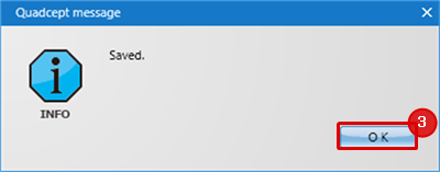
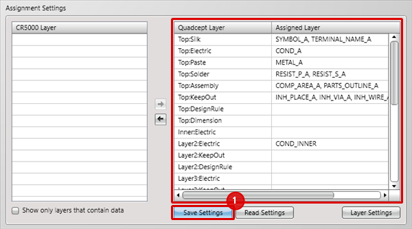
| The assignment information can be saved. |
| (1) |
Click the "Save Settings" button. |
|
 |
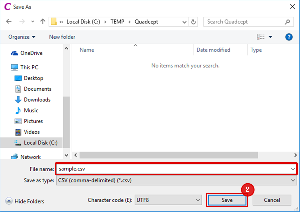
| (2) |
After entering its file name, click the "Save" button. |
|
 |
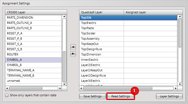
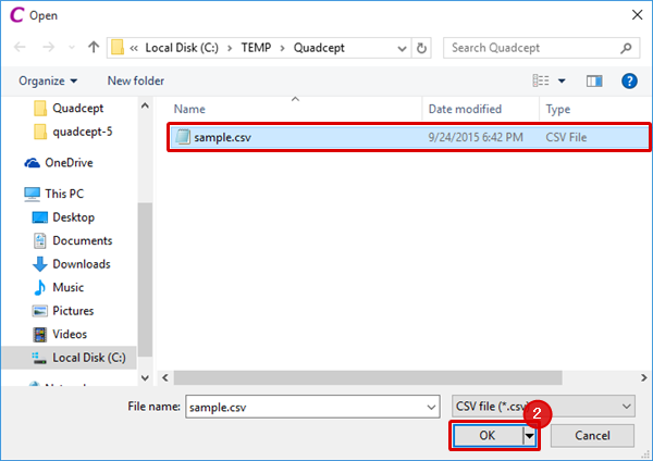
| The saved assignment settings can be read. |
| (1) |
Click "Read Settings". |
|
 |
| (2) |
Select an assignment settings file and then click the "OK" button. |
|
 |
| |
The assignment settings are read. |
|
 |
| |
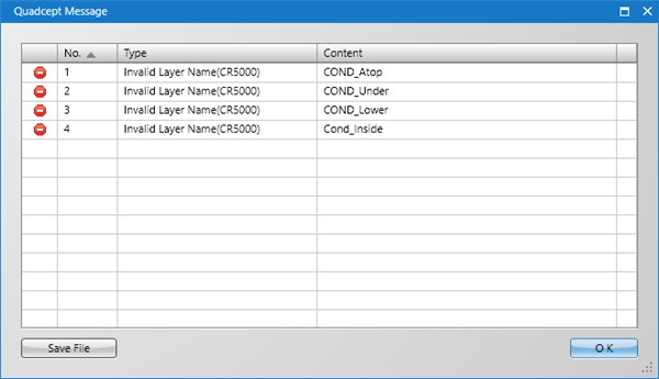
*Messages appear if there is no corresponding layer in a ftf file or on the Quadcept Layer when reading assignment settings. |
|
 |
Layer Settings
If you want to edit the Quadcept Layer when assigning layers, configure its settings from "Layer Settings".
In regard to its settings, refer to Layer of PCB Settings.