

PCB Layout CAD : Design Preparation
Layer Settings
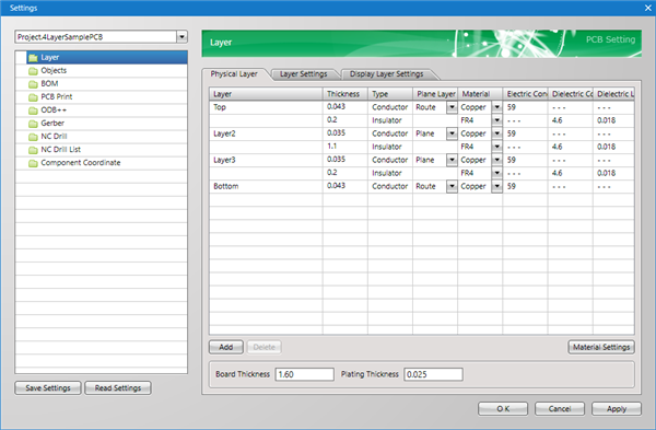
Before proceeding with PCB design, first configure Board Layer Settings for the design that you are making this time.
With Layer Settings, set the number of physical board layers, add Customize layers, layer color, and Display Layer Settings etc.
Number of Board Layers
For single-surface boards and double-surface boards, there are two layers; the Top Layer and Bottom Layer.
When there is a conductor layer inside of the board in addition to the surface layer, add an inner layer.
| Layer Settings |
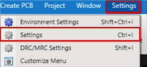
| Layer Settings can be configured from "Layer" in PCB Settings. |
|
 |
|
 |
The following will explain about "2-Layer Boards" and "4-Layer Boards".
2-Layer Boards
Delete Physical Layers and leave the "Top" and "Bottom" layers
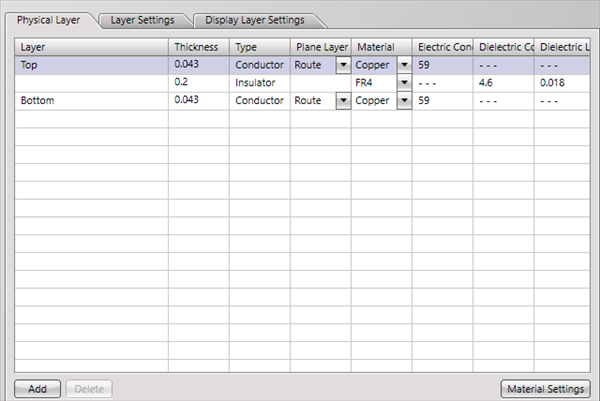
4-Layer Boards
Add Physical Layers so that there are four layers; "Top", "Layer2", "Layer3", and "Bottom

Adding Customize Layers
Next, configure Customize Layer settings.
Customize layers can be added for each Physical Layer (Top, Inner, and Bottom) and Other layers (Whole).
Add arbitrary necessary layers such as Dimensions, Alignment Marks, Comments, and V Cut Instructions.
| Adding Customize Layers and Layer Settings |
|
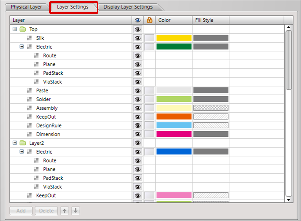 |
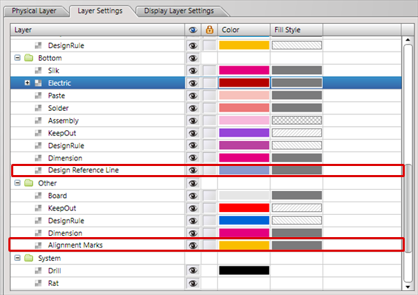
Addition Example
Arbitrary layers such as for "Design Reference Line" and "Alignment Marks" are added.
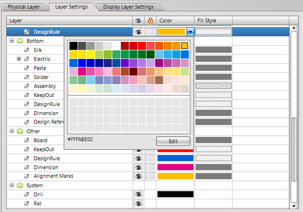
Configure Layer Color Settings
Next, configure Color settings.
By clicking on a color, you can select a color from the color palette. You can select any color you want.
For more details about this screen, refer to "Layer" in PCB Setting.
Changing the Color
Click "Color" to open the Color Palette, and then select a color.
Configure Display Layer Settings
Next, "Display Layer Settings" will be explained.
With "Display Layer Settings", it is possible to register the layers that will be displayed on the PCB design screen using the Batch List of the "Display List".
This setting can be called from the "Read Display Layer Settings (Batch List)" box of the "Layer" window while designing a PCB.
| Display Layer Settings |
|
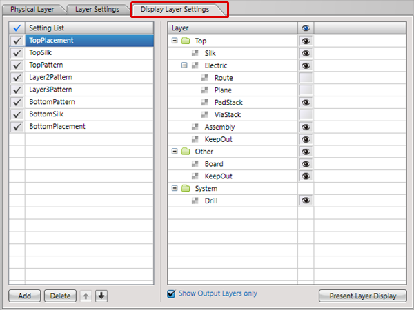 |
By pressing the "Present Layer Display" button, the current layer display status on the PCB screen can be imported to the settings.