

PCB Layout CAD : PCB Settings
Layers
Configure layer settings for PCB documents. In the Layer setting dialog, it is possible to configure "Physical Layer", "Layer Settings" and Display Layer Settings.
| Item | Description |
|
Configures electrical layers such as Top and Bottom layers. |
|
|
Customize layers such as layers for Dimensions and layers for comments can be added to Physical Layers. |
|
|
Toggling can be done easily by registering display of the PCB drawing that is being designed. |
For more details about opening the PCB Settings screen, refer to About PCB Settings.
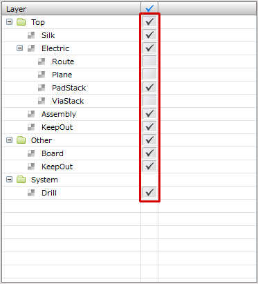
Layer Screen
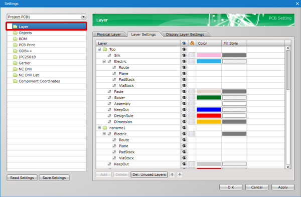
Explanation of Layers
| Layers | Description |
|
Top, Bottom |
Indicates the Top layer(Component side) and Bottom layer(Solder side). (These cannot be deleted because they are predetermined layers.) |
|
noname |
Indicates an added inner signal layer. Its layer name can be changed. |
|
Other |
Common layers such as Board (Board Outline) for all layers. |
|
System |
Layer used for the system such as Drills and Rats. (These cannot be added or deleted because they are predetermined layers.) |
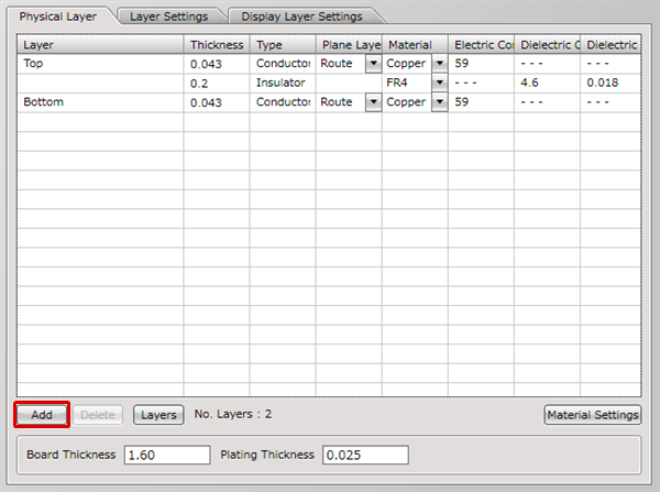
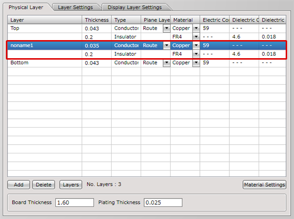
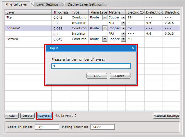
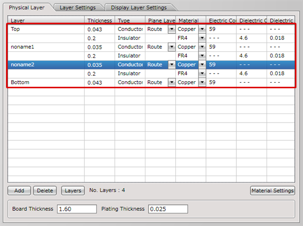
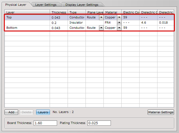
Physical Layer
Configure Physical Layer settings.
For a 2-layer board, configure settings for the "Top" and "Bottom" layers.
For a 4-layer board, configure settings for the "Top", "Layer2", "Layer3", and "Bottom" layers.
Thickness and materials, etc., are used for Recommended Width (Impedance Control).
When not necessary, etc., it is OK not to configure these settings.
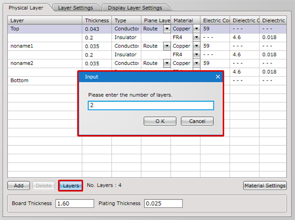
| Adding Physical Layers |
| The following will explain how to add physical layers. |
|
 |
|
 |
|
 |
|
 |
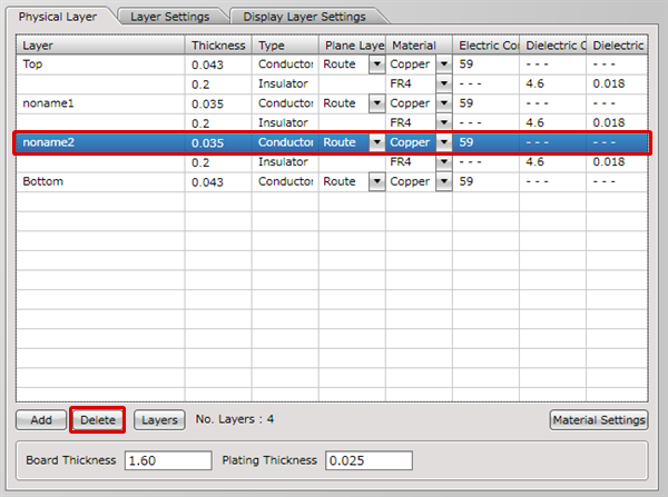
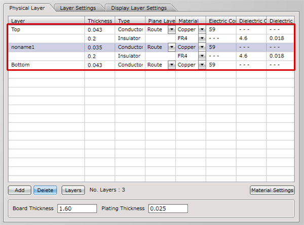
| Deleting Physical Layers |
| The following will explain how to delete physical layers. |
|
 |
|
 |
|
 |
|
 |
It is also possible to add/delete layers while designing. However, when deleting an added layer,
it is necessary to delete all objects placed on that layer.
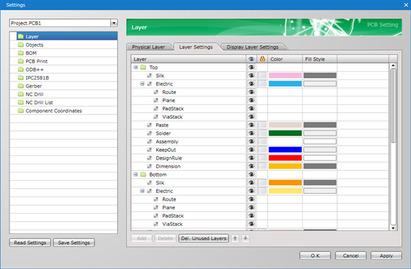
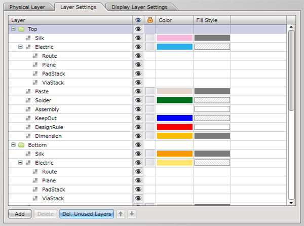
Layer Settings
It is possible to configure customize layers included in each layer and color settings.
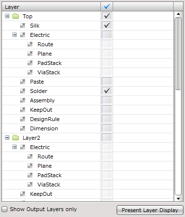
For surface layers (Top/Bottom), "Silk", "Electric", "Paste", "Solder", "Assembly", "KeepOut", "DesignRule", and "Dimension" layers are automatically prepared.
When a Physical Layer is added to an inner layer, an "Electric", "KeepOut", and "DesignRule" layer are created automatically.
For Other layers, "Board", "KeepOut", "DesignRule", and "Dimension" layers are prepared.
For System layers, "Drill", "Rat", "ConnectionPoint", "DRC/MRC Error", "DRC/MRC Error(Approved)", "Background Color", "Cursor", "Selected Item", "Grid", and "Origin Point" are prepared.
In addition to the above, it is possible to add customize layers (Dimension, Comment, Assembly Drawing) freely.
Explanation of Default Layers
The following will explain the default layers that are prepared automatically.
Default layers cannot be deleted.
| Layers | Description |
|
Silk |
This is the Silk object layer, and it includes Non-Electric Objects such as References, Lines, and Text. |
|
Electric |
This is the Copper layer, and electric objects such as Routes, Planes, Pad Lands, and Via Lands are automatically included in this "Electric" layer. |
|
Route |
This is the Route object layer in the Electric layer. |
|
Plane |
This is the Plane object layer in the Electric layer. |
|
PadStack |
This is the Pad Land object layer in the Electric layer. |
|
ViaStack |
This is the Via Land object layer in the Electric layer. |
|
Paste |
This is the metal mask and paste mask layer. When metal mask settings are configured for the CHIP pad, |
|
Solder |
This is the solder resist and solder mask layer. When Solder Resist Settings are configured for a Pad/Via, |
|
Assembly |
This is the official outline line layer for components. For IPC Footprints, official outline lines for components are created in this layer automatically. It is also possible to prepare this when creating a footprint. |
|
KeepOut |
This is the Keep Out Area layer. When this setting is configured for individual layers, it is created in the KeepOut layer of each layer. When common for all layers, it is created in the KeepOut layer for Other. |
|
DesignRule |
This is the Design Rule Area layer. When this setting is configured for individual layers, it is created in the DesignRule layer of each layer. When common for all layers, it is created in the DesignRule layer for Other. |
|
Dimension |
This is the Dimension layer. For "Create Component Dimension Automatically", by default, dimensions are automatically created in the Dimension layer. For "Create Board Outline Dimension Automatically", by default, dimensions are automatically created in the Dimension layer for Other. |
|
Board |
This is the Board Outline layer. A closed drawing is drawn using Lines and Arcs, etc. |
System Layer
| Layers | Description |
|
Drill |
The color of the Drill on the board can be set. Drills created using Pads and Vias are recognized automatically. |
|
Rat |
The color settings for Lines (Rats Net) that express Net connections can be configured. |
|
ConnectionPoint |
The color settings for Connection Point objects can be configured. |
|
DRC/MRC Error |
The color of DRC/MRC error marks can be configured. The color of error marks for "Not yet" errors is set by this setting. |
|
DRC/MRC Error(Approved) |
The color of DRC/MRC error marks can be configured. The color of error marks for "Approved" errors is set by this setting. |
|
Background Color |
Background Color settings can be configured. |
|
Cursor |
The color of the Cursor Shape can be set. |
|
Selected Item |
The color can be set for when an object is selected. |
|
Grid |
GRID Line color settings can be configured. |
|
Origin Point |
Origin Point Mark Color settings can be configured. |
Item
| Item | Content |
|
Display Mark |
You can toggle display ON/OFF. |
|
Lock Mark |
Layer objects can be locked. It becomes impossible to select objects placed on locked layers. |
|
Color |
By clicking on a color, you can select a color from the color palette. You can select any color you want. |
|
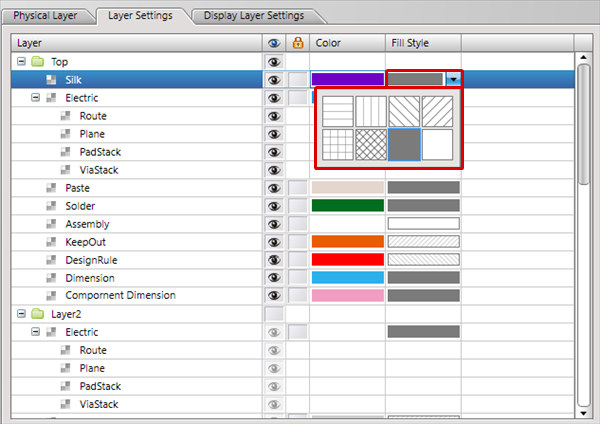
Fill Style |
The Fill Type can be selected. |


- Use Toggle All ON/OFF to easily turn display and the lock mark ON/OFF.
- It is possible to change the order in the same Physical Layer, and the display order changes according to this order. The higher it is displayed, the higher the display priority.
The following will explain various operations that can be executed from the Layer Settings window.
- Adding a Customize Layer
- Deleting a Customize Layer
- Changing the Name of a Customize Layer
- Changing Each Layer Color
- Changing the Fill Style of Each Layer
- Deleting All Unused Layers
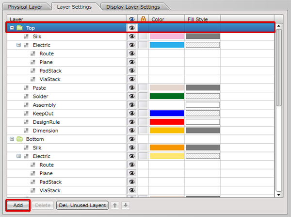
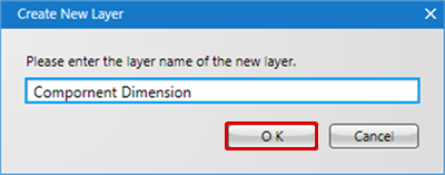
| Adding a Customize Layer |
| The following will explain how to add a customize layer. |
|
 |
|
 |
| Deleting a Customize Layer |
| The following will explain how to delete a customize layer. |
|
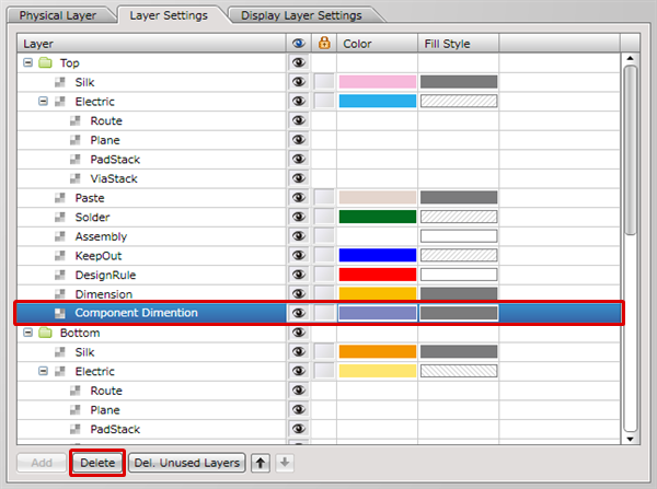 |
| Changing the Name of a Customize Layer |
| The following will explain how to rename a customize layer. |
|
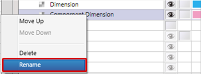 |
| Changing Each Layer Color |
| The following will explain how to change the color of each layer. |
|
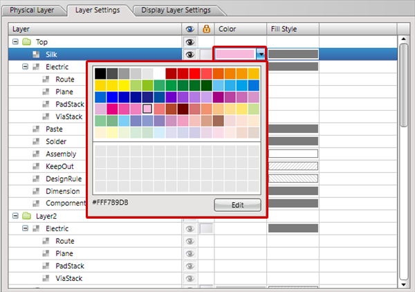 |
|
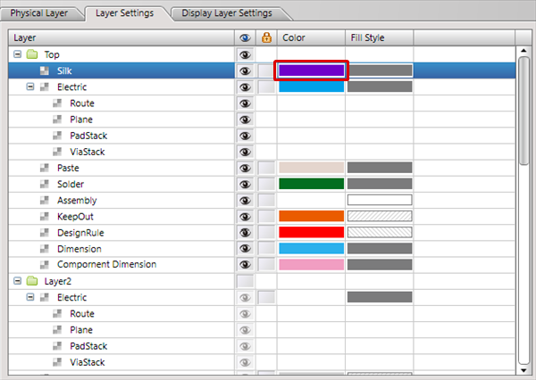 |
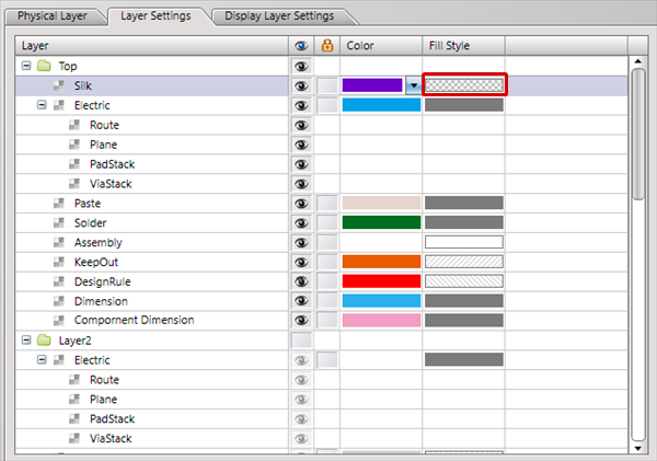
| Changing the Fill Style |
| The following will explain how to change the Fill Style of each layer. |
|
 |
|
 |
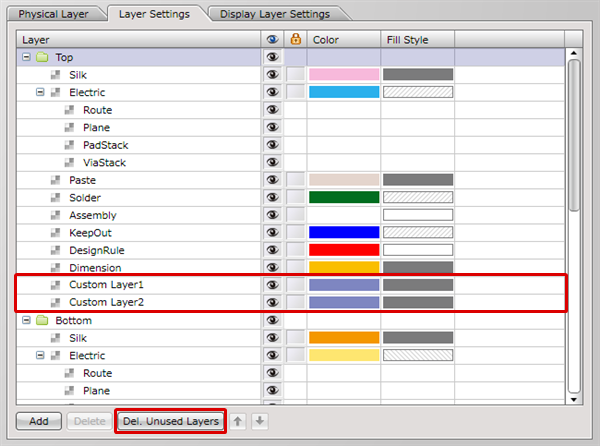
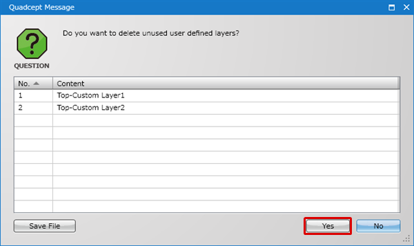
| Deleting All Unused Layers |
| It is possible to delete all unused customize layers with no objects placed. The following will explain how to delete all unused layers. |
|
 |
|
 |
|
 |
|
 |
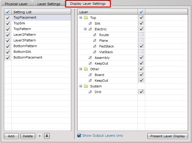
Display Layer Settings
By registering display of the PCB drawing that is being designed, you can easily toggle from the Layer Window or from the bottom of the screen.
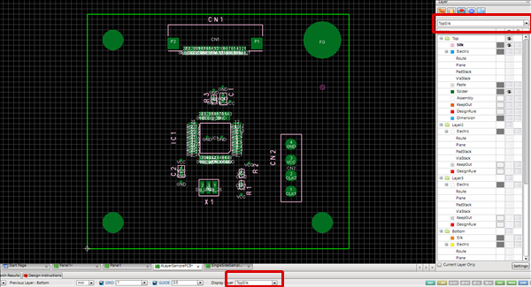
Refer to Reading Display Layer Settings.
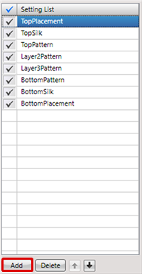
| Adding to the Setting List |
| The following will explain how to add to the Setting List. |
|
 |
|
 |
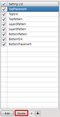
| Deleting from the Setting List |
| The following will explain how to delete from the Setting List. |
|
 |
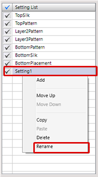
| Changing Names in the Setting List |
| The following will explain how to change names in the Setting List. |
|
 |
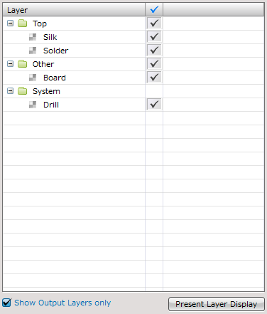
Show Output Layers only
When the check for "Show Output Layers only" is removed, all layers will be shown.
| When "Show Output Layers only" is checked | When "Show Output Layers only" is unchecked |
|
|
|
Present Layer Display
The Display Layer that applies to the current design drawing can be applied automatically.
This is convenient because confirmed settings displayed on the screen can be applied as they are.
Saving Settings
Settings can be saved and read. For more details, refer to Default Environment.