

Quadcept : Creating Components
Creating Components
Create components that are placed on schematics and PCB design drawings.
The difference with symbols is that component information and internal attributes can be defined and registered.
In addition, for components, symbols (schematic component shapes) and footprints (PCB component shapes) can be prepared in advance, and link registration is possible.
Also, footprints can automatically be referenced and placed when transferring Net Information from a schematic to a PCB.
For an overview of components, refer to About Components.
The following is the procedure for creating components.
STEP 1: Open the Create New Screen for a Component
STEP 2: Configure Reference Settings
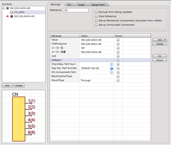
STEP 3: Input Attributes
STEP 4: Register Symbols (Circuit Component Shapes)
STEP 5: Confirm Pin Assignment
STEP 6: Register Footprints (PCB Component Shapes)
STEP 7: Confirm Pin Settings
STEP 8: Register Swap Information
STEP 9: Save
For more details, refer to Creation Method Flow.
Create Component Screen
Create Component Screen
Creation Method Flow
The following is the procedure for creating components.
|
STEP 1: Open the Create New Screen for a Component As the first operation, open a Create New screen for a component. |
↓
|
STEP 2: Configure Reference Settings A Reference is text for identifying a component. Ex.) U1, R1, C1, Q1... |
↓
|
Attributes refer to the setting operation for information related to components such as the Rated value, Multiplier factor, and Maker. (10V, 50V, 250V, 10K) |
↓
|
STEP 4: Register Symbols (Circuit Component Shapes) Register symbols (circuit component shapes). (* If you do not design schematics, this is not necessary.) |
↓
|
STEP 5: Confirm Pin Assignment Make adjustments for when the Symbol Pin No. and Component Pin No. are different. If the Symbol Pin No. and component are the same, you can move to the next step. |
↓
|
STEP 6: Register Footprints (PCB Component Shapes) Register footprints (PCB component shape). (* If you do not design PCBs, this is not necessary.) |
↓
|
Configure pin settings. You can configure setting for "Pin No.", "Pin Name", "Toggle Display", "Electrical Characteristics", and "Non Connection". |
↓
|
STEP 8: Register Swap Information Configure Swap Pin and Group Swap settings. (* If there is no need to swap, it is possible to skip this item.) |
↓
|
Save the component file. |
The following will explain the operation flow using the following components.
Sample: Creating a Zener Diode
Sample: Creating an IC (Gate/Alternate Component)