In Quadcept, after designing a schematic and executing Transfer to PCB, component placement work for the PCB can be done while confirming the schematic.
| The following will explain the component placement operation for PCBs while confirming a schematic. |
| (1) |
Open the schematic that is the target for placing components to the PCB. |
| (2) |
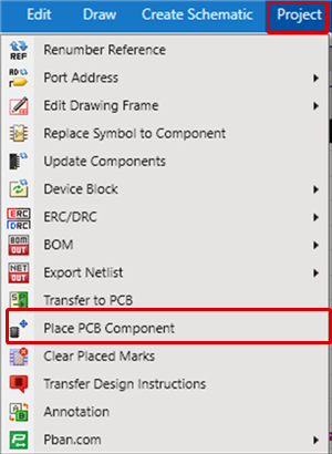
Select [Project]
=> [Place PCB Component].
=> It will move to Place PCB Component mode. |
|
 |
| (3) |
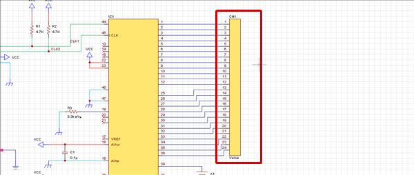
Click the component on the schematic for which you want to execute Place PCB Component.
|
|
 |
| (4) |
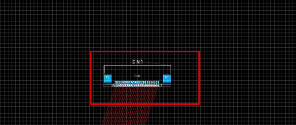
It will automatically move to the PCB screen and change to Placement mode.
=> Click on an arbitrary location to complete placement.
|
|
 |
| (5) |
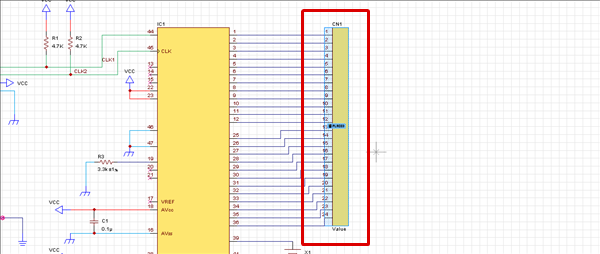
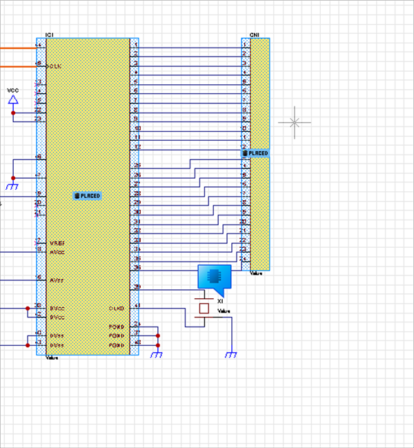
After placement is complete, it will automatically return to the schematic, and a "Placed Mark" will be displayed.
=> You can visually confirm which components have already been placed.
|
|
 |
If there are multiple PCB sheets in a project, it is possible to select the target PCB sheet.
Clearing Place Component Marks
| Before Clearing |
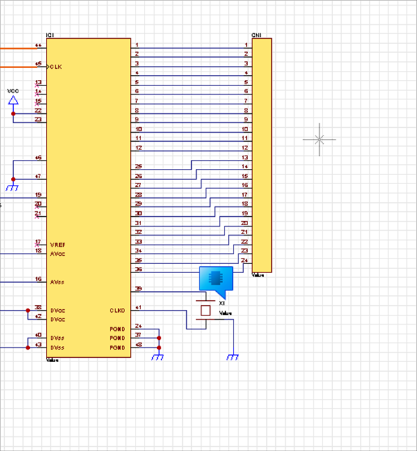
After Clearing |
|
|
|
When you place a component using [Place PCB Component], a "Placed Mark" is displayed on the schematic.
The following will explain how to clear "Placed Marks". |
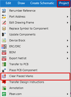
| (1) |
Select [Project]
=> [Clear Placed Marks]. |
|
 |
| |
Placed marks will be cleared. |
|
 |