
Quadcept : About Quadcept
Overall Flow
The following will explain the overall flow from circuit design to PCB design.
| Schematic Design |
| Place component symbols, connect wires, and create an electronic/electrical circuit drawing. Connection information can be linked with post-process printed circuit board design (artwork). |
|
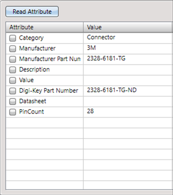
Prepare data for the drawing frame and components required for the design.
|
|
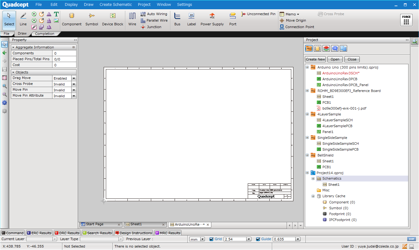
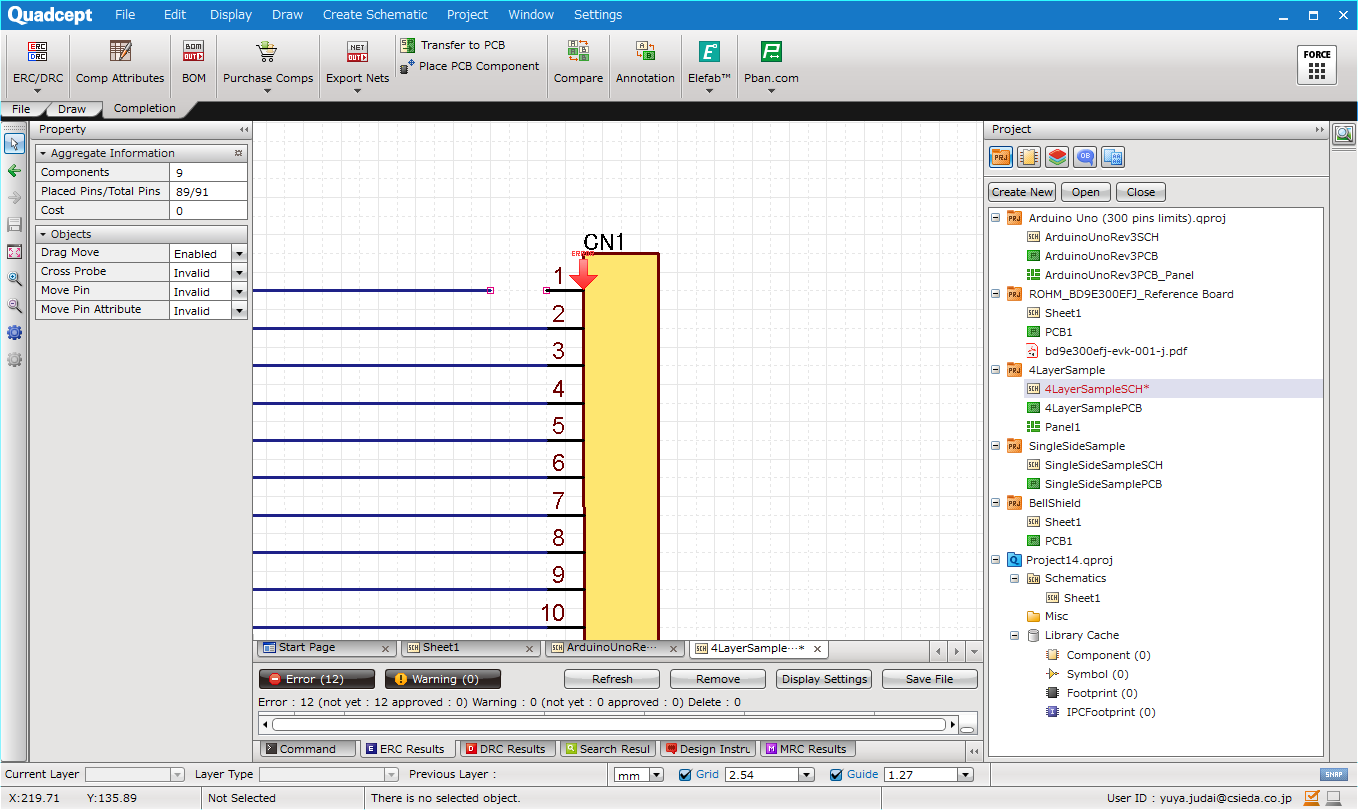
First, create a new project and circuit drawing for the schematic design.
|
|
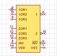
Place components on the drawing.
|
|
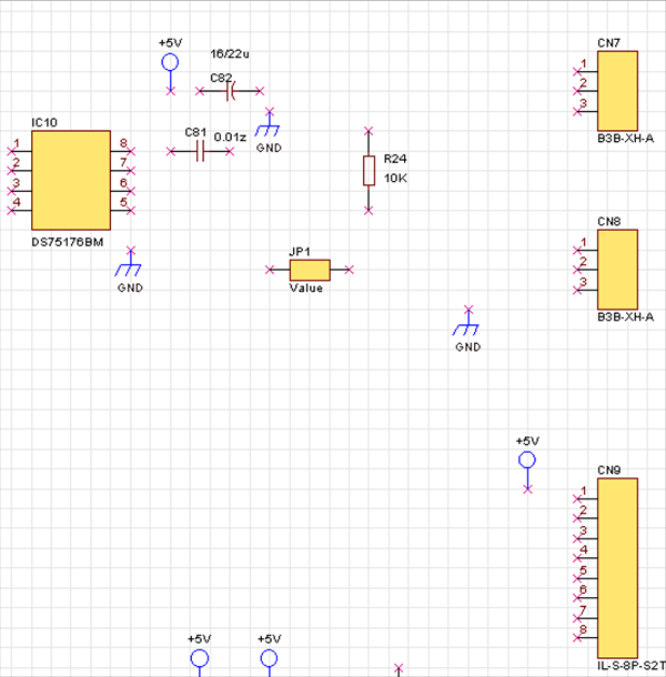
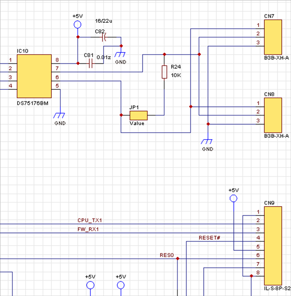
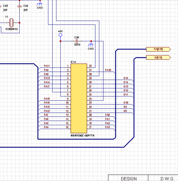
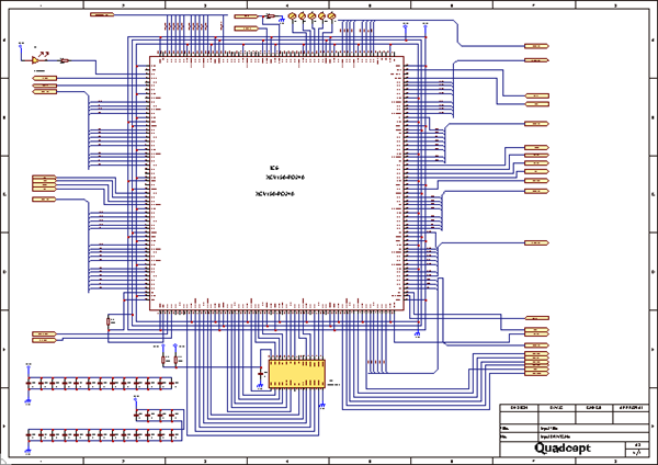
Connect wires, and draw the schematic.
|
|
Check whether there are any problems with the schematic connections or display. |
|
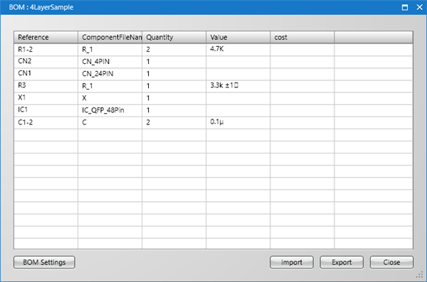
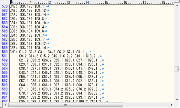
Print the Netlist, BOM, and drawing, and the schematic creation is complete.
|
| Printed Circuit Board Design |
| Based on the connection information and components designed in the schematic, create a pattern for a printed circuit board. |
|
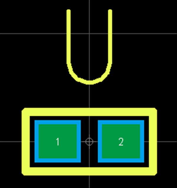
Prepare data for the footprints and components required for the design.
|
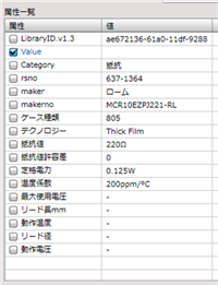
|
First, create a new project and PCB drawing for the PCB design.
|
|
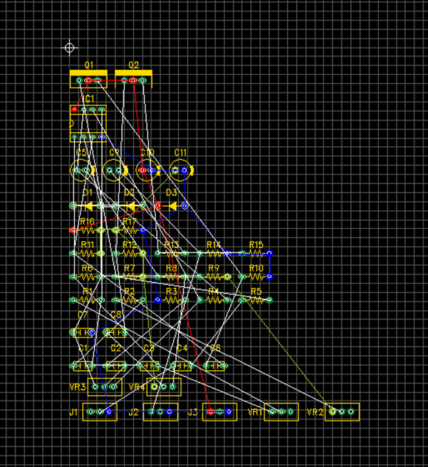
Read the component and connection information designed on the schematic.
|
|
As preparation for designing, configure design rules such as the number of layers and the route width.
|
|
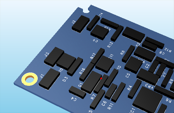
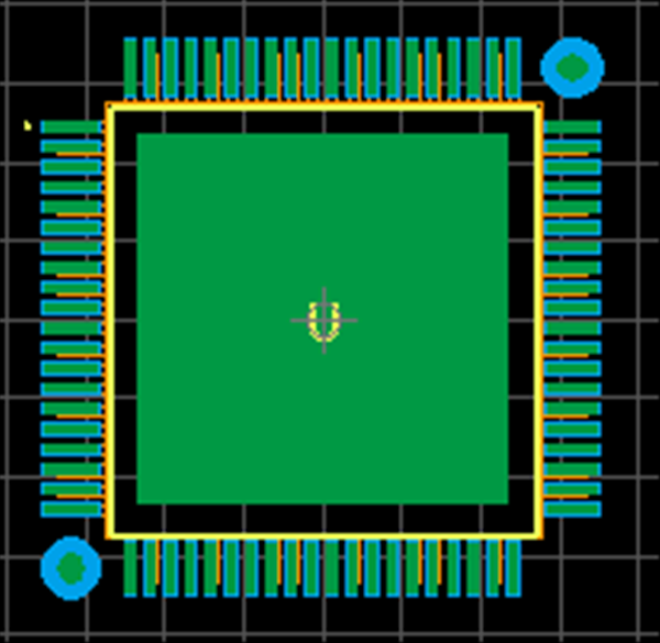
Consider the component electromagnetic characteristics, thermal characteristics, I/O signal level, and frequency, and execute placement so that routing will be easier to perform later.
|
|
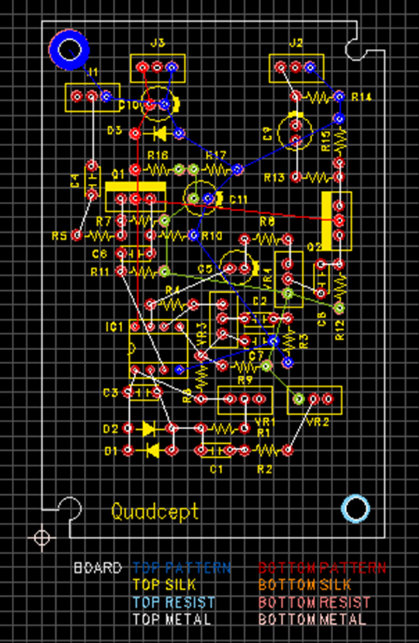
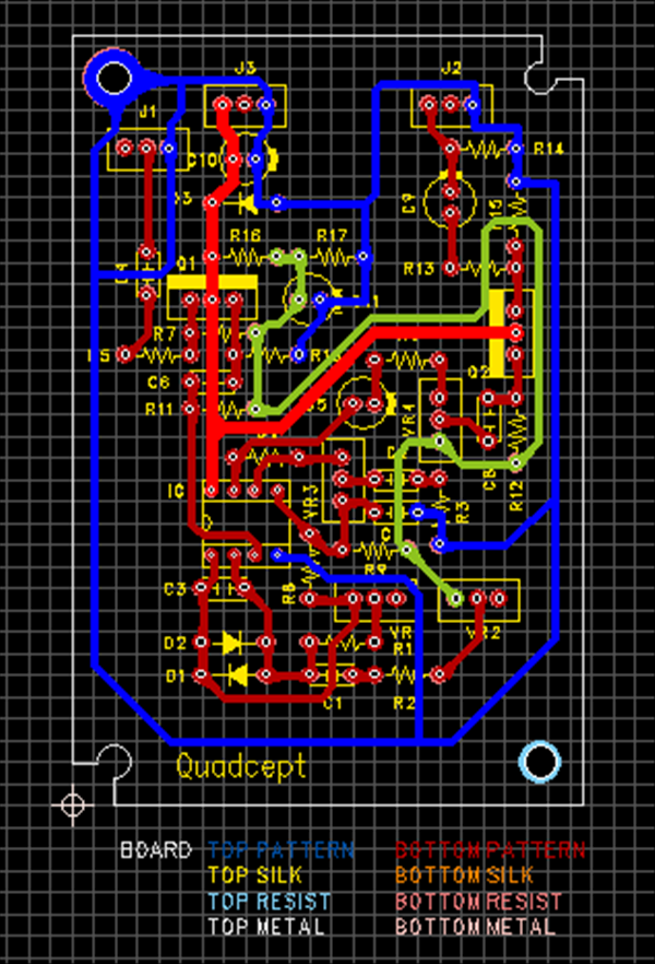
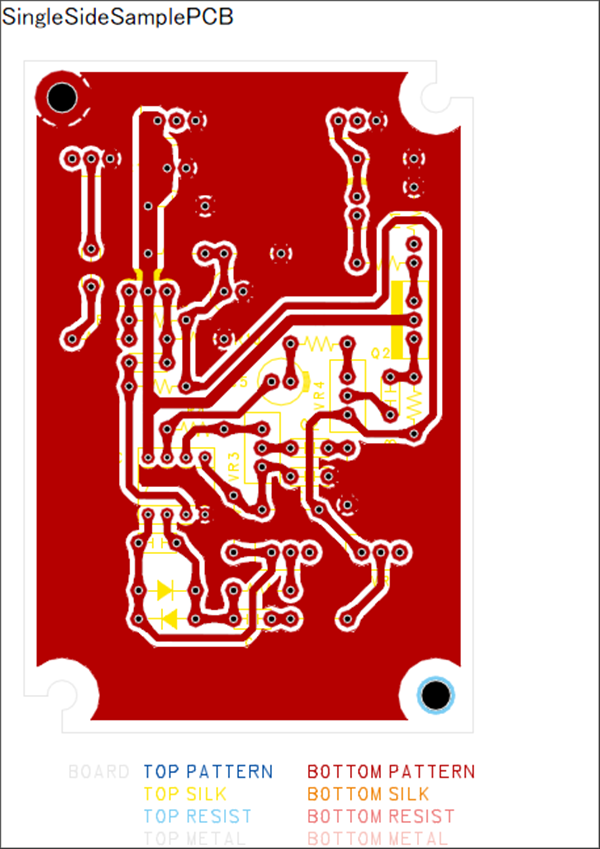
Execute routing by considering the current capacity and impedance, etc.
|
|
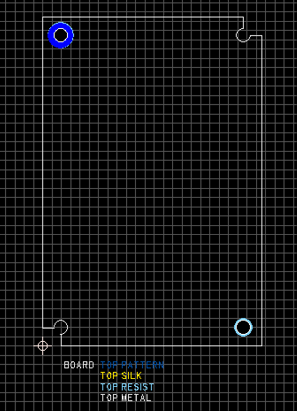
After completing board routing, fill the gaps in the pattern with planes (copper).
|
|
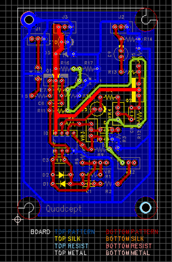
Check whether there are any design rule violations with the printed circuit board design.
|
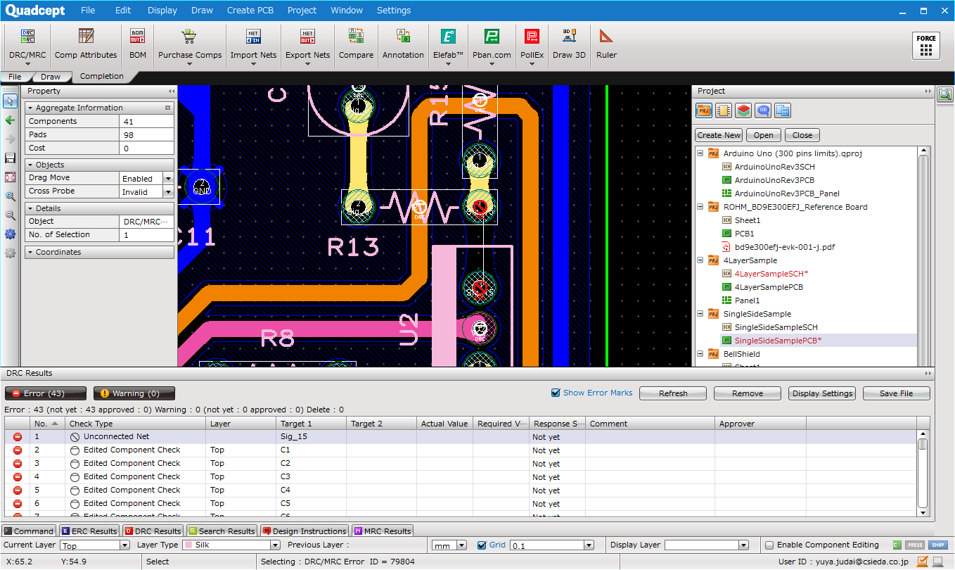 gn rule violations with the printed circuit board design.
|
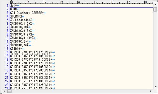
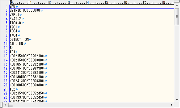
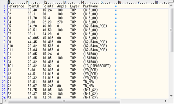
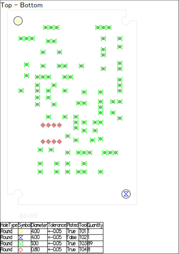
Perform export of various files for board manufacturing from the completed printed circuit board design.
|
|
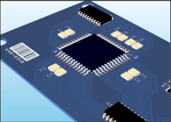
Confirm the printed circuit board design using 3D display, and export it as a 3D file for linking with the 3D tool.
|