

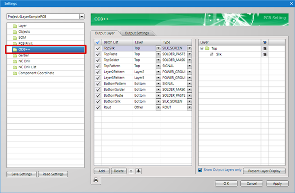
PCB Layout CAD : PCB Settings
ODB++
This a setting for outputting ODB++ files in PCB documents.
ODB++ stands for Open Data Base, and it is a data format for executing PCB design and data exchange among mounting companies.
It covers necessary information exchanged for CAD, CAM, and DFM from PCB design to manufacturing, and it contains more information than a Gerber, so problems due to lack of information or recognition errors will not occur.
The display layer for exported ODB++ files can be set in advance.
For more details about opening the PCB Settings screen, refer to About PCB Settings.
| Tab Items | Content |
|
Display layer combinations for Export ODB++ can be registered. |
|
|
Export items for exporting ODB++ files can be set. |
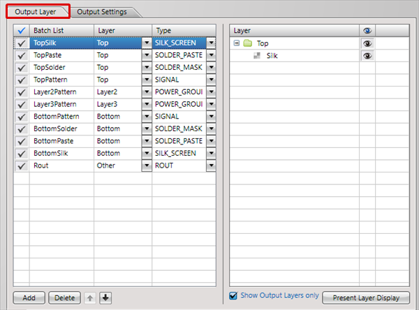
Output Layer
Display layer combinations for Export ODB++ can be registered.
The checks on the left toggle between Enabled/Invalid. Uncheck temporarily unnecessary items for exporting.
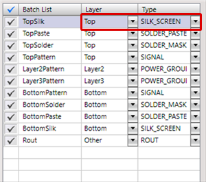
Example of Batch List Settings
With TopPattern, only "Electric" of the Top Layer is exported as the display status.
For others such as TopSilk, all can be exported according to the display combination set in the Display Settings.
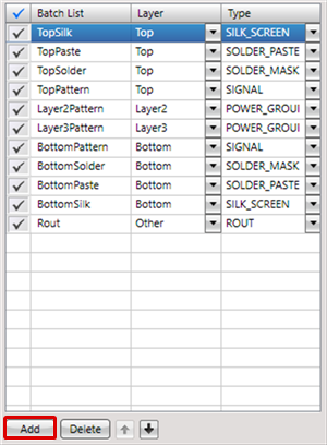
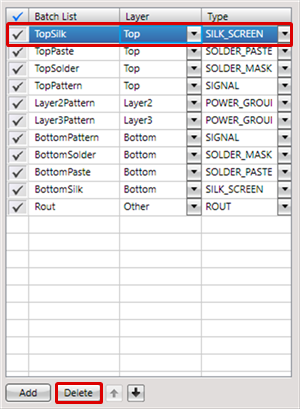
| Adding to the Batch List |
| The following will explain how to add to the Batch List. |
|
 |
|
 |
|
 |
About Layer and Type
For ODB++, you must set the "Layer" and "Type".
Assign a Physical Layer for Layer.
Select and set a Type from the following Types.
Type List
| Types of Types | Content |
|
SILK_SCREEN |
Silk data layer |
|
SOLDER_PASTE |
Paste mask layer |
|
SOLDER_MASK |
Solder mask layer |
|
SIGNAL |
Signal line layer |
|
POWER_GROUND |
Power supply layer |
|
MIXED |
Mixed layer with signal lines and power supplies |
|
ROUT |
Layer for Board Outlines and boards with large holes |
|
DOCUMENT |
Layer for various information |
| Deleting from the Batch List |
| The following will explain how to delete from the Batch List. |
|
 |
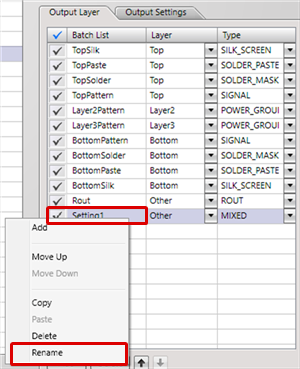
| Changing Names in the Batch List |
| The following will explain how to change names in the Batch List. |
|
 |
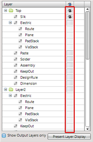
Show Output Layers only
When the check for "Show Output Layers only" is removed, all layers will be shown.
| When "Show Output Layers only" is checked | When "Show Output Layers only" is unchecked |
|
|
|
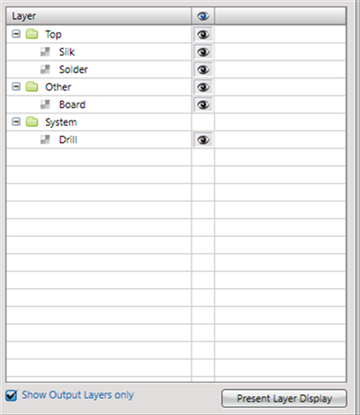
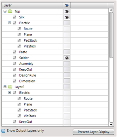
Present Layer Display
The Display Layer that applies to the current design drawing can be applied automatically.
This is convenient because confirmed settings displayed on the screen can be applied as they are.
About Layer and Type Settings
With ODB++ format, it is necessary to distinguish layers such as Top and Bottom, and types such as Silk Screen, Solder Mask, and Solder Paste.
Select the proper Layer and Type from the list.
Output Settings
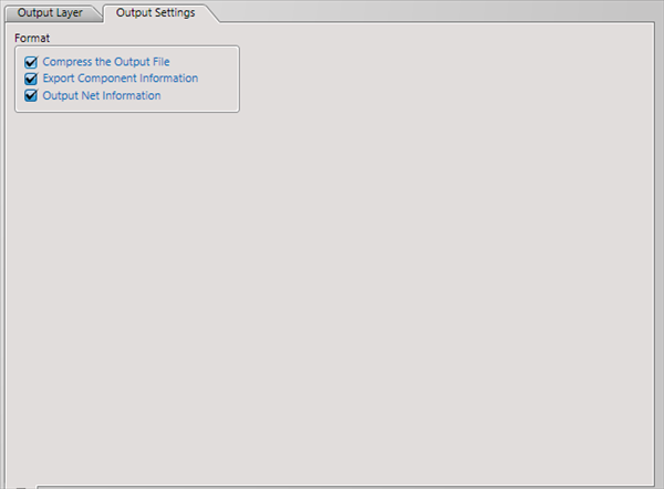
Export contents for exporting ODB++ files can be set.
| Item | Content |
|
Compress the Output File |
Compresses the ODB++ file as a Zip file, and saves it. |
|
Export Component Information |
Also exports Mounted Component Information (including coordinates/shapes) in the ODB++. |
|
Output Net Information |
Outputs Net Connection information in the ODB++. |
Executing Export ODB++
There are the following methods for executing Export OBD++.
- Click the "*****" icon of the ODB++ screen of the PCB Settings
- Open a PCB document, [Project] => [ODB++] => [Export ODB++]
- Batch Output
Saving Settings
Settings can be saved and read. For more details, refer to Default Environment.