With Quadcept, it is possible to transfer differences due to design changes in schematic/PCB data.
The following will explain Forward Annotation and Backward Annotation for when transferring design changes.
To execute Annotation, it is necessary to match "References" between a schematic and PCB, or to match "Component IDs".
* To perform Annotation (transfer/compare differences) for a “Reference”, it is necessary to match "Object IDs", which is the standard.
* "Component IDs" are the unique ID for each component.
<Forward Annotation>
| Design changes to schematics |
Transfer Differences => => |
Reflected to PCB |
|

|
 |

|
<Back Annotation>
| Design changes to PCB |
Transfer Differences => => |
Reflected to schematic |
|

|
|

|
|
The following will explain how to transfer design change contents from the schematic side to PCB data.
|
| (1) |
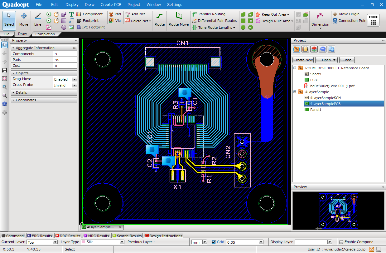
Open the updated file (the file you want to be reflected).
=> For Forward Annotation, open PCB data. |
|
 |
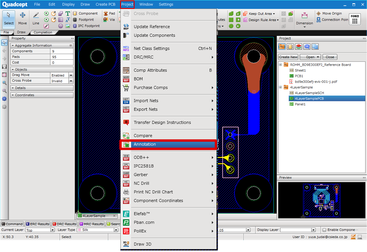
| (2) |
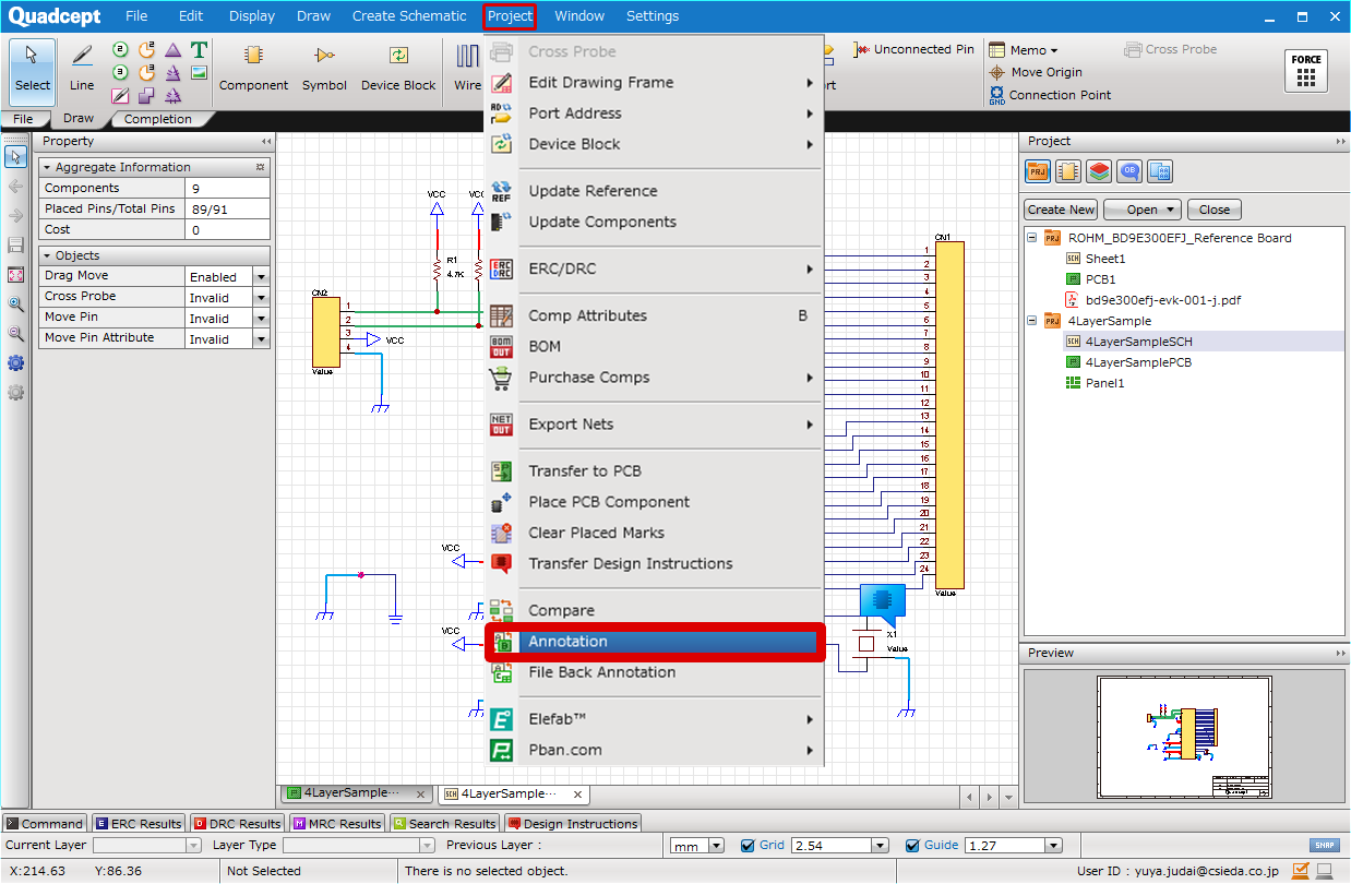
[Project]
Select => [Annotation]
=> The Select target screen will open. |
|
 |
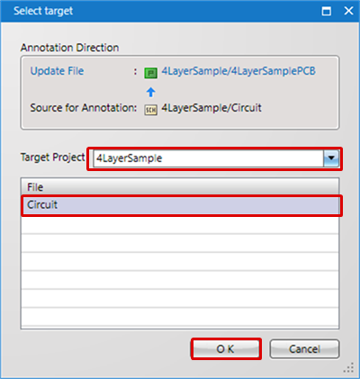
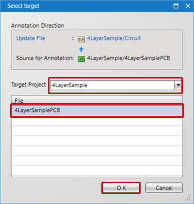
| (3) |
Select a Source for Annotation (Target Project and File), and click "OK"
=> To select a schematic, select "Circuit". All schematics in the Project will be targeted. |
| |
* When multiple Projects are registered, it is possible to select other projects by switching the Target Project.
|
|
 |
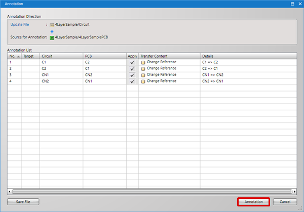
| (4) |
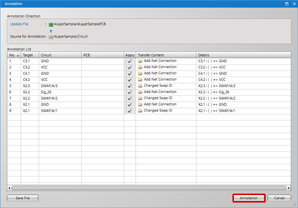
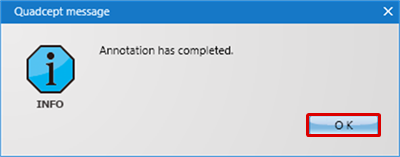
The Annotation screen will open showing the contents of the differences. Confirm the contents, and then click "Annotation".
=> The contents with the Apply checkbox "ON" will be reflected to the PCB data. |
| |
* With Forward Annotation, updates other than for Net (Add Component and Edit Attribute, etc. ) are performed first, and then updates for the Net (Edit Net Name, Add Net Connection, etc. ) are performed.
* For more information about content details, see here. |
|
 |
| (5) |
Contents of the differences between the schematic and PCB will be reflected to the PCB side. |
|
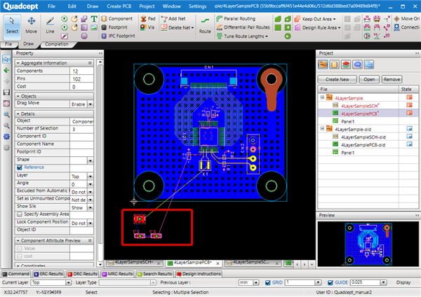 |
When a component is newly added, the conditions are the settings in "Align Footprint".
Components that are newly added by forward annotation have a "NEW" icon, which makes them easy to identify.
|
The following will explain how to transfer design change contents from the PCB side to the schematic.
|
| (1) |
Open the updated file (the file you want to be reflected).
=> For Back Annotation, open schematic data. |
|
 |
| (2) |
[Project]
Select => [Annotation]
=> The Select target screen will open. |
|
 |
| (3) |
Select a Source for Annotation (Target Project and File), and click "OK" |
| |
* When multiple Projects are registered, it is possible to select other projects by switching the Target Project. |
|
 |
| (4) |
The Annotation screen will open showing the contents of the differences. Confirm the contents, and then click "Annotation".
=> The contents with the Apply checkbox "ON" will be reflected to the schematic data. |
| |
* For more information about content details, see here.
*Please note that "Change Net Connection", "Add Net Connection" and "Delete Net Connection" are not reflected to schematics by back-annotation. |
|
 |
| (5) |
The contents of the differences between the schematic and PCB will be reflected to the schematic side. |
|
 |