
PCB Layout CAD : Panelize (Imposition)
Panelization
A panel sheet allows defining a panel of the same or different board designs.
| Panelization |
|
|
Things that are Imported for Panelization
For panelizing PCBs, there is various work such as adding waste boards, creating router/perforation/V-Cut , and placing fiducial marks.
Quadcept delivers strong support to make it easy to panelize PCBs.
- Waste Board
Generally, the width is approximately 10 mm. For waste boards, planes are placed for each layer in order to suppress board warpage.
- Router/Perforation/VCut
Router/Perforation/VCut, etc., are added so that the board can be divided into single products.
- Fiducial Mark (Also referred to as a Recognition Mark)
This is used for alignment when mounting components. These are placed diagonally or at the four corners of the board.
- Location Hole
A Non Through Hole with a diameter of φ3.0 to 4.0 at the edge of waste boards. It is used when setting a location pin to a component mounted device.
- Alignment Mark (Also referred to as a Reference Mark, etc.)
This is used for alignment and for confirming size.
- Board Outline Text
Text placed for each layer and displayed when executing Gerber Print, etc. This is used for confirming Gerber data.
Panelization
The following explains various operations related to panelization.
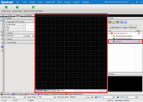
Creating Panel Sheets
Placing Panels
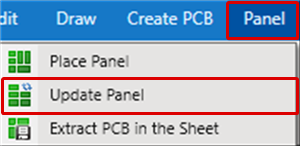
Updating Panels
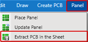
Extracting PCBs from Panels
Creating Panel Sheets
A panel sheet can be created in the following two ways.
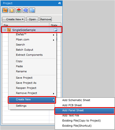
Adding a Panel Sheet into an Existing Project
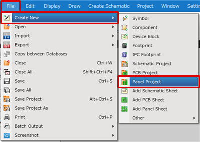
Creating a New Panel Project
| Adding a Panel Sheet into an Existing Project |
| The following explains how to add a panel sheet to an existing project. |
|
 |
|
|
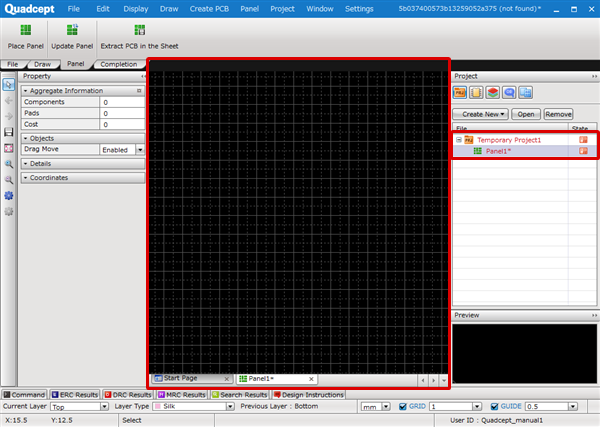
| Creating a New Panel Project |
| The following explains how to add a panel sheet by creating a panel project. |
|
 |
|
 |
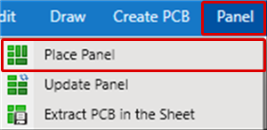
Place Panel
The following explains how to place a board to a panel sheet.
| Place Panel |
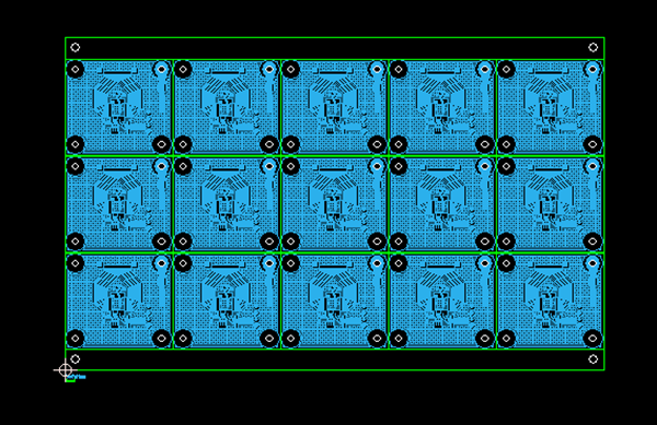
| The following explains how to define the board array and place the boards on a panel sheet. A panel is organized by selecting a PCB file and configuring the panelization settings such as the number of boards, angle and spacing. * You can define a panel of different board designs by repeating this operation. |
|
 |
|
 |
For the "Waste Board" portion, same as for the PCB Sheet, an arbitrary shape can be created as a "Board Outline" on the Panel Sheet.
Place Panel Screen Description
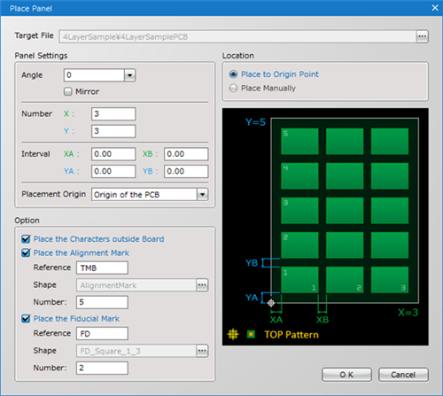
Target File
| Item | Content |
|
Target File |
Click "..." to select the source PCB Sheet for executing Panelize (Imposition) to the Panel Sheet. |
Panel Settings
| Item | Content |
|
Angle |
Specifies the angle of the PCB (Panel) placed on the Panel Sheet. |
|
Mirror |
Specifies mirror for the PCB (Panel) placed on the Panel Sheet. |
|
Number |
Specifies the number of placed PCBs (Panels) in the X Axis/Y Axis directions. |
|
Interval |
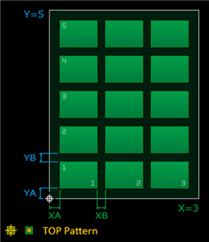
Specifies the Interval from the Origin Point to the Placement Origin (XA/YA) and the Interval between PCBs (Panels) (XB/YB).
|
|
Placement Origin |
Specifies the position of the PCB (Panel) as the Origin Point for aligning with the Panel Sheet Origin Point. |
Option
| Item | Content |
|
Place the Characters outside Board |
Specifies whether to place text for each layer that is displayed when executing Gerber Print, etc. |
|
Place the Alignment Mark |
Places alignment marks on a panel sheet. When checking the checkbox, the following settings will be enabled. |
|
Place the Fiducial Mark |
Places fiducial marks on a panel sheet. When checking the checkbox, the following settings will be enabled. |
Location
| Item | Content |
|
Location |
Specifies either "Place to Origin Point" or "Place Manually" (placed at an arbitrary position using the mouse) for the previous setting. |
| Update Panel |
| The following explains how to perform "Update Panel" to reflect design changes made on a source board in the panel. |
|
 |
|
|
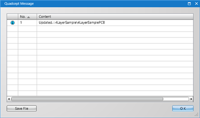
If design changes are found on a source board when opening a panel sheet, a message will appear to confirm whether to reflect the changes in the panel. You can also update the panel by selecting "Yes" for that message.
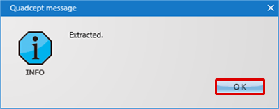
| Extract PCB in the Sheet |
| The following explain how to perform "Extract PCB in the Sheet" to extract PCB designs placed on a panel sheet. The extracted PCB will be added as a PCB sheet to the same project. By saving PCB designs with this command, you will be able to edit the designs even when you do not have its source PCB data. |
|
 |
|
|