

PCB Layout CAD : Various Convenient Functions
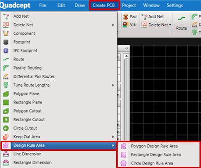
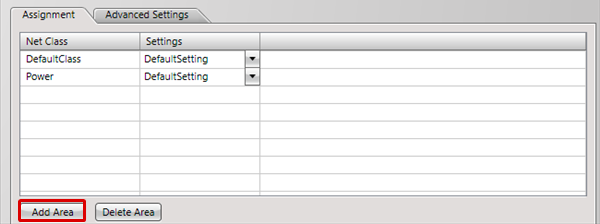
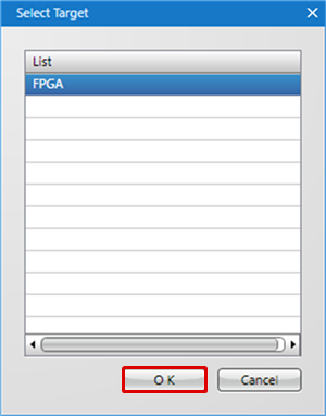
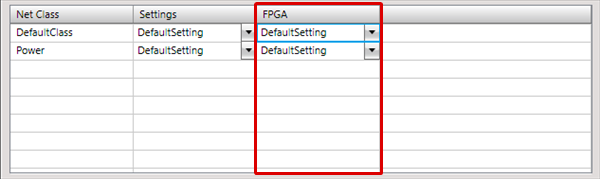
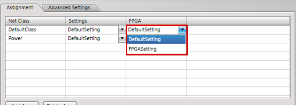
Various Design Rule Areas
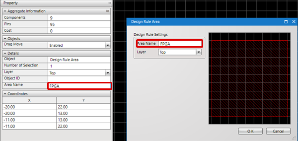
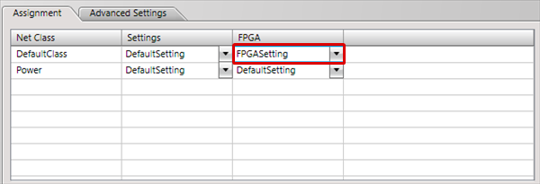
For Design Rule Areas, when the Design Rules are not for the whole board in the DRC Settings items and they differ according to the layer and area, it is possible to set areas and define them separately.
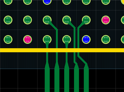
This is used for locations with narrow pitch such as connectors and FPGAs, and for locations that require primary side creeping distance with the power supply circuit.
Items for which the Design Rules can be Set according to the Design Rule Area
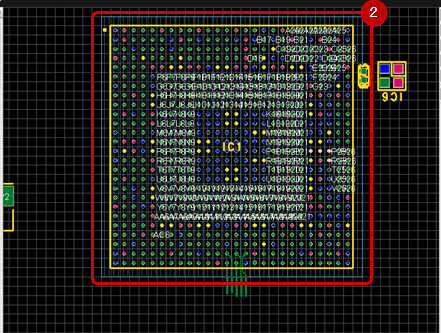
For objects that are targets of the Design Rule Area, the applicable condition is "Completely in the Rule Area".
Clearance
Route
Tear Drop
Dynamic Plane Connection
| Methods for Using the Design Rule Area |
| Design Rule Area Drawing Method and Method for Setting DRC according to the Design Rule Area |
|
 |
|
 |
|
 |
|
 |
|
 |
|
 |
|
 |
|
 |