

PCB Layout CAD : DRC/MRC Settings
Component Clearance
Check Clearance Violations between components and component Assembly Areas.
For the Assembly Area, the area of the Assembly Area during footprint creation is the check target.
When the area of the Assembly Area is not created during footprint creation, a Rectangle Assembly Area is automatically created using Component Silk and Pad Position, and this becomes a check target.
It is possible to confirm the Assembly Area by placing a check for the component "Specify Assembly Area" setting and displaying the "Assembly" layer.
For more details about opening the DRC/MRC Settings screen, refer to About DRC/MRC Settings.

Example Clearance Settings
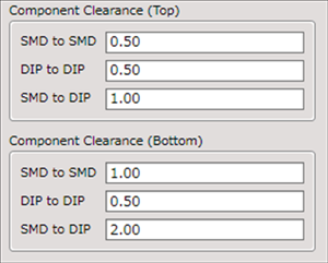
Component Clearance (Top), Component Clearance (Bottom)
Check the Clearance between components.
Surface Mounted Component = Components including SMD Pads (Footprint)
Insertion Mounted Component = Components without SMD Pads (Footprint)
| Item | Content |
|
SMD to SMD |
Checks the Clearance between SMDs. |
|
DIP to DIP |
Checks the Clearance between DIPs. |
|
SMD to DIP |
Checks the Clearance between SMDs and DIPs. |
Input a negative number (such as -1) for items that you want to place outside the check target.